NVMe IP Core (Gen4) for AG5 Reference Design Manual
3.1 Test Firmware (nvmeiptest_ag5.c)
3.2 Function List in Test Firmware
1 Overview
NVM Express (NVMe) is a specification that defines the interface between the host controller and solid-state drive (SSD) through PCI Express. It optimizes the process of issuing commands and completions by utilizing only two registers (Command issue and Command completion), and enables parallel operation by supporting up to 64K commands within a single queue. This improves transfer performance for both sequential and random access operations.
In the PCIe SSD market, two standards are commonly used: AHCI and NVMe. AHCI is an older standard designed for SATA hard disk drives while NVMe is optimized specifically for non-volatile memory such as SSDs. For a detailed comparison between the AHCI and NVMe protocols, refer to the document titled “A Comparison of NVMe and AHCI” available at https://sata-io.org/system/files/member-downloads/NVMe%20and%20AHCI_%20_long_.pdf
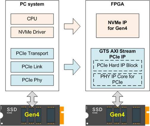
Figure 1 NVMe Protocol Layer
To access an NVMe Gen4 SSD, a typical system employs an NVMe driver running on a processor, as shown on the left side of Figure 1. The physical connection between the host and the NVMe device is made via a PCIe connector, which follows a one-to-one connection model, meaning that each PCIe host connects directly to a single PCIe device without requiring a PCIe switch.
The NVMe-IP implements the NVMe driver entirely in hardware logic, allowing access to NVMe SSDs without the need for a processor or software-based drivers. By integrating NVMe-IP into an FPGA, the system eliminates the overhead associated with software-hardware communication, resulting in higher performance for both write and read operations with NVMe SSDs.
2 Hardware
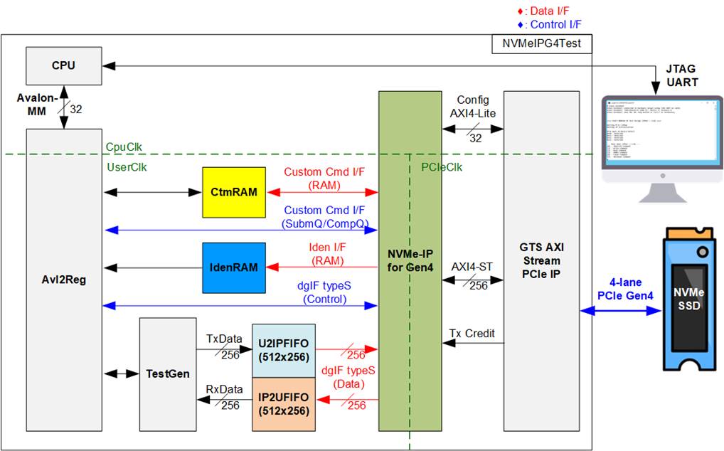
Figure 2 NVMe-IP for Gen4 Demo Hardware
The hardware modules in the test system are divided into three main parts: the test function (TestGen), the NVMe function (comprising CtmRAM, IdenRAM, U2IPFIFO, IP2UFIFO, NVMe-IP for Gen4, and the PCIe block), and the CPU system (including CPU and Avl2Reg).
The TestGen module interfaces with the NVMe-IP for Gen4’s user interface and is responsible for generating the data stream for Write commands and verifying the data stream of Read commands. The write and read data streams are stored in two FIFOs (U2IPFIFO and IP2UFIFO). TestGen continuously writes or reads data when the FIFO is ready, ensuring optimal transfer performance for system evaluation.
The NVMe function includes the NVMe-IP for Gen4 and the PCIe Hard IP (GTS AXI Stream PCIe IP), enabling direct access to an NVMe Gen4 SSD without PCIe switch connection. The command requests and parameters for each command, which are inputs to the NVMe-IP for Gen4, are controlled by the CPU through the Avl2Reg module. Additionally, the data interface for both Custom and Identify commands connects to RAMs accessible by the CPU.
The CPU is connected to the Avl2Reg module, interfacing with the NVMe test logic. Integrating the CPU into the test system allows users to set test parameters and monitor the status via a JTAG UART. The CPU also facilitates the execution of multiple test cases to verify the functionality of the NVMe-IP. The default firmware for the CPU includes functions for executing NVMe commands using the NVMe-IP for Gen4.
Figure 2 illustrates three clock domains used in the design: CpuClk, UserClk, and PCIeClk.
· CpuClk: Dedicated clock domain for the CPU, its peripherals, and the AXI4-Lite configuration interface of the PCIe. It is generated from a stable clock source that is independent of other hardware components.
· UserClk: Used for the operation of the NVMe-IP for Gen4, RAM, and TestGen modules. According to the NVMe-IP for Gen4 datasheet, the UserClk frequency must be equal to or greater than PCIeClk. In this design, UserClk is set to 275 MHz (≥ 250 MHz).
· PCIeClk: Generated by the PCIe Hard IP to synchronize data streams over 256-bit AXI4-Stream. It operates at 250 MHz for 4-lane PCIe Gen4 configuration.
Further hardware details are provided in the subsequent sections.
2.1 TestGen
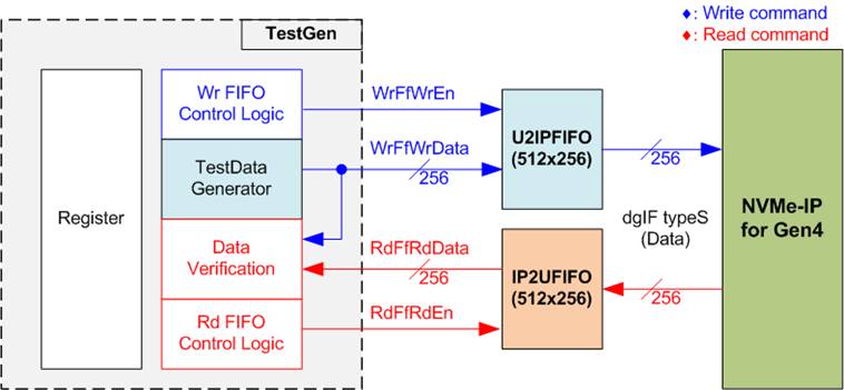
Figure 3 TestGen Interface
The TestGen module manages the data interface of the NVMe-IP, facilitating data transfer for both Write and Read commands. During a Write command, TestGen generates 256-bit test data and sends it to NVMe-IP via U2IPFIFO. In contrast, for a Read command, the data is received from IP2UFIFO and compared against the expected value to ensure data accuracy. TestGen’s data bandwidth is set to match the NVMe-IP, running at the same clock and using the same data bus size to optimize performance.
TestGen’s control logic ensures that the Write or Read enable is asserted to 1b whenever the corresponding FIFO is ready to transfer data. This allows both U2IPFIFO and IP2UFIFO to be ready for data transfer to and from the NVMe-IP, achieving optimal write and read performance with the SSD.
The module provides flexibility by allowing the user to configure test parameters through the console, including the start transfer address, total transfer size, transfer direction, and test pattern selector. These parameters are stored in the Register block. The detailed hardware logic of TestGen is illustrated in Figure 4.
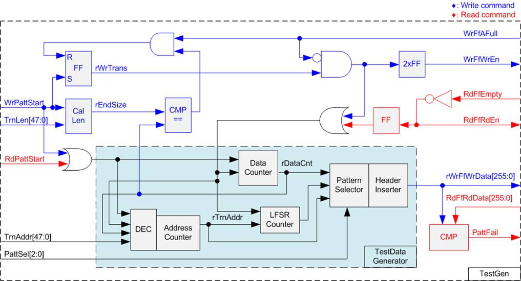
Figure 4 TestGen Hardware
In Figure 4, two key aspects of the system are depicted. The first part (upper section) illustrates the control of data flow, while the second part (lower section) details the generation of test data for use with the FIFO interface.
In the upper section of Figure 4, we focus on the control of data flow. Two signals, the WrFfAFull and RdFfEmpty, are integral to the FIFO interface for flow control. When the FIFO reaches its capacity (indicated by WrFfAFull=1b), the WrFfWrEn signal is set to 0b, effectively pausing data transfer into the FIFO. In a read operation, when data is available within the FIFO (indicated by RdFfEmpty=0b), the system retrieves this data for comparison by setting the RdFfRdEn to 1b. Furthermore, it is important to note that both write and read operations are completed when the total transferred data matches the user-defined value. Consequently, the counter logic is designed to track the amount of data transferred during this command, and upon command completion, both WrFfWrEn and RdFfRdEn must be de-asserted.
The lower section of Figure 4 outlines the methods for generating test data, either for writing to the FIFO or for data verification. There are five available test patterns: all-zero, all-one, 32-bit incremental data, 32-bit decremental data, and LFSR. These patterns are selected by the Pattern Selector.
For the all-zero or all-one pattern, every bit of the data is set to zero or one, respectively. In contrast, the other test patterns are designed by splitting the data into two parts to create unique test data within every 512-byte data block, as shown in Figure 5.
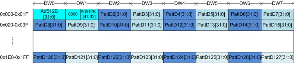
Figure 5 Test Pattern Format for Increment/Decrement/LFSR Patterns in Each 512-Byte Data Block
Each 512-byte data block consists of a 64-bit header in Dword#0 and Dword#1, followed by the test data in the remaining words (Dword#2 – Dword#127). The header is generated using the address in 512-byte units (rTrnAddr), controlled by the Address counter block. The initial value of the address counter is set by the user (TrnAddr) and increases after transferring each 512-byte block.
The content of the remaining Dwords (DW#2 – DW#127) depends on the pattern selector, which could be 32-bit incremental data, 32-bit decremental data, or LFSR pattern. The 32-bit incremental data is designed using the Data counter, while the decremental data can be created by connecting a NOT operation to the incremental data. The LFSR pattern is generated using the LFSR counter, using the equation x^31 + x^21 + x + 1.
To generate 256-bit test data for the LFSR pattern, the data is split into two 128-bit sets, each with a different start value, as illustrated in Figure 6.
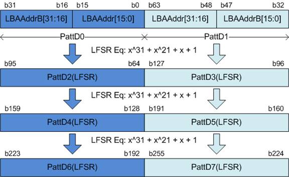
Figure 6 256-bit LFSR Pattern in TestGen
Using a look-ahead technique, each clock cycle generates four 32-bit LFSR values or 128-bit data, represented by the same color in Figure 6. The start value of each data set is derived from a combination of the 32-bit LBAAddr and the NOT operation applied to specific bits of the LBAAddr (LBAAddrB), creating unique start values for each 128-bit data set. The generated test data is either written to the FIFO as write data or used as expected data for verification against the read data from the FIFO. If a mismatch occurs during data verification, the failure flag is set to 1b.
The timing diagram for writing data to the FIFO is outlined below.
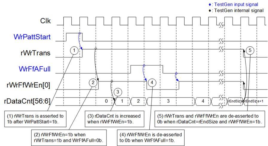
Figure 7 Timing Diagram of Write Operation in TestGen
1) The write operation is initiated by asserting WrPattStart signal to 1b for a single clock cycle, which is followed by the assertion of rWrTrans to enable the control logic for generating write enable to FIFO.
2) If two conditions are satisfied (rWrTrans is asserted to 1b during the write operation and the FIFO is not full, indicated by WrFfAFull=0b), the write enable (rWrFfWrEn) to FIFO is asserted to 1b.
3) The write enable is fed back to the counter to count the total data transferred during the write operation.
4) If FIFO is almost full (WrFfAFull=1b), the write process is temporarily paused by de-asserting rWrFfWrEn to 0b.
5) The write operation is completed when the total data count (rDataCnt) matches the set value (rEndSize). At this point, both rWrTrans and rWrFfWrEn are de-asserted to 0b.
For read transfer, the read enable of FIFO is controlled by the empty flag of FIFO. Unlike the write enable, the read enable signal is not stopped by total data count and not started by start flag. When the read enable is asserted to 1b, the data counter and the address counter are increased to count the total amount of data and generate the header of expected value, respectively.
2.2 NVMe
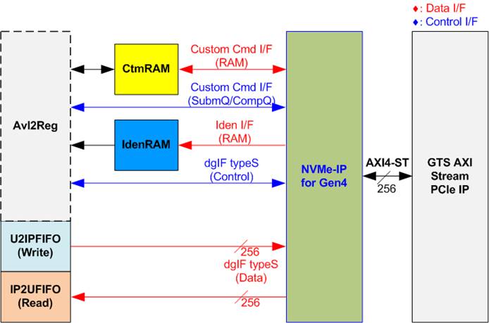
Figure 8 NVMe Hardware
In the reference design, the NVMe-IP’s user interface consists of a control interface and a data interface. The control interface receives commands and parameters from either the Custom command interface or the dgIF typeS interface, depending on the type of command. For instance, the Custom command interface is used for operating SMART, Secure Erase, or Flush command.
In addition, the data interface of NVMe-IP has four different interfaces with a data bus width of 256-bit. These interfaces include Custom command RAM interface (bi-directional), Identify interface (unidirectional), FIFO input interface (dgIF typeS and unidirectional), and FIFO output interface (dgIF typeS and unidirectional).
In the reference design, the Custom command RAM interface is typically used for one-way data transfer, such as when the NVMe-IP sends SMART data to the Avl2Reg module.
2.2.1 NVMe-IP for Gen4
The NVMe-IP implements the NVMe protocol on the host side, enabling direct access to an NVMe Gen4 SSD without PCIe switch connection. It supports seven commands: Write, Read, Identify, Shutdown, SMART, Secure Erase, and Flush. Further details about the NVMe-IP can be found in the datasheet.
https://dgway.com/products/IP/NVMe-IP/NVMe-IP-g4-datasheet-ag5/
According to the NVMe-IP for Gen4 datasheet, the latency between the FIFO Read Count signal and the FIFO Read Enable signal must be exactly one clock cycle. Therefore, in this reference design, both U2IPFIFO and IP2UFIFO are implemented using synchronous FIFOs generated by the IP catalog to ensure the required one-clock-cycle latency.
2.2.2 GTS AXI Stream PCIe IP
The GTS AXI Stream PCIe IP is a Hard IP block integrated in Altera FPGAs, responsible for implementing the Physical, Data Link, and Transaction Layers of the PCIe specification. More information is available in the following document:
https://docs.altera.com/r/docs/813754/current
2.2.3 Two-port RAM
Two of two-port RAMs, CtmRAM and IdenRAM, store the returned data from Identify and SMART commands, respectively. IdenRAM is simple dual-port RAM with one read port and one write port and has a data size of 8 Kbytes to store the 8 Kbyte output from the Identify command.
The data bus size for NVMe-IP and Avl2Reg differ, with NVMe-IP having a 256-bit size and Avl2Reg having a 32-bit size. As a result, IdenRAM is an asymmetric RAM with different bus sizes for its Write and Read interfaces.
The NVMe-IP also has a double-word enable, which allows it to write only 32-bit data in certain cases. The RAM setting on the IP catalog enables write byte enable, so each bit of the double word enable is extended to a 4-bit write byte enable, as shown in Figure 9.
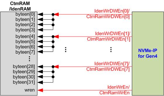
Figure 9 Byte Write Enable Conversion Logic
Each bit of WrDWEn is extended to be 4-bit of IdenWrEn, so bit[0], [1], ..., [7] are then used to drive bits[3:0], [7:4], …, [31:28] of IdenWrEn, respectively.
On the other hand, CtmRAM is implemented as a two-port RAM with two read ports and two write ports, and with byte write enable. The connection from the double-word enable of NVMe-IP to byte enable of CtmRAM is similar to that of IdenRAM. The two-port RAM is utilized to support additional features when the customized Custom command requires data input. While a simple dual-port RAM would be sufficient to support the SMART command, which returns only 512 bytes of data, CtmRAM is implemented with an 8KB capacity to accommodate customized Custom command requirements.
2.3 CPU and Peripherals
The CPU system uses a 32-bit Avalon-MM bus as the interface to access peripherals such as the Timer and JTAG UART. The system also integrates an additional peripheral to access the NVMe-IP test logic by assigning a unique base address and address range. To support CPU read and write operations, the hardware logic must comply with the Avalon-MM bus standard. Avl2Reg module, as shown in Figure 10, is designed to connect the CPU system via the Avalon-MM interface, in compliance with the standard.
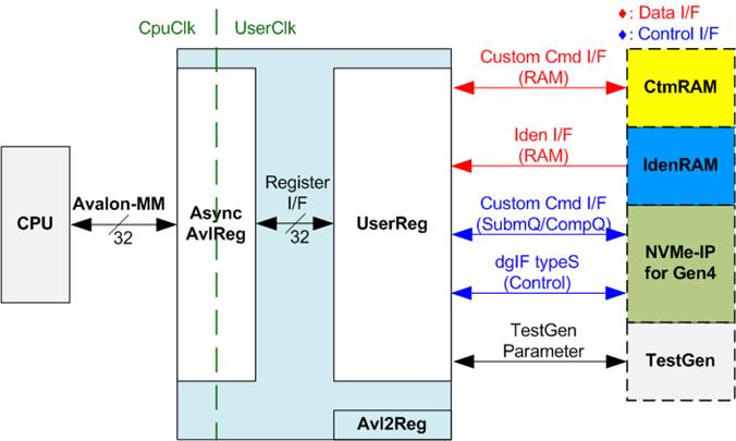
Figure 10 CPU and Peripherals Hardware
Avl2Reg consists of two main components: AsyncAvlReg and UserReg. AsyncAvlReg converts the Avalon-MM signals into a simple Register interface with a 32-bit data bus size, matching the Avalon-MM data bus size. It also incorporates asynchronous logic to handle clock domain crossing between the CpuClk and UserClk domains.
UserReg contains the register file for parameters and status signals from other modules in the test system, including the CtmRAM, IdenRAM, NVMe-IP, and TestGen. The details of AsyncAvlReg and UserReg are explained further below.
2.3.1 AsyncAvlReg
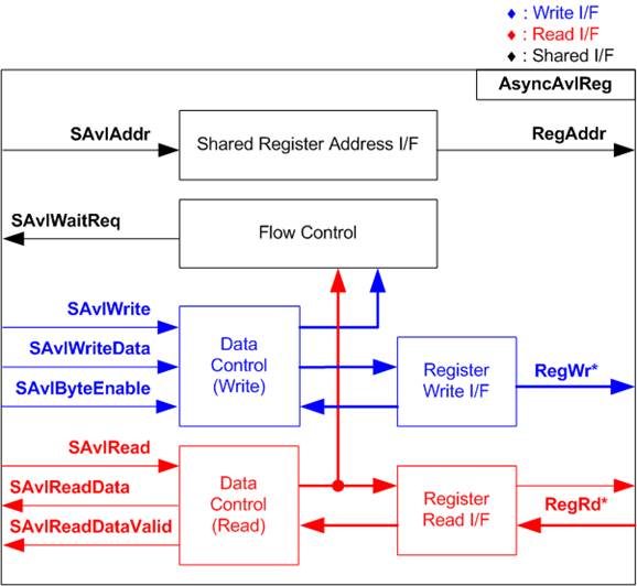
Figure 11 AsyncAvlReg Interface
https://docs.altera.com/r/docs/683091/current
According to the Avalon-MM specification, only one command (write or read) can be executed at a time. AsyncAvlReg’s logic is organized into three groups: Write control logic, Read control logic, and Flow control logic. The flow control logic asserts SAvlWaitReq to hold off subsequent requests from the Avalon-MM interface until the current request completes. Write control and Write data signals of the Avalon-MM bus are latched and transferred to the Write register interface through clock domain crossing registers. Similarly, Read control signals are latched and transferred to be Read register interface. Afterward, the data returned from Register Read I/F is transferred back to Avalon-MM bus using clock domain crossing registers. The Address I/F of Avalon-MM is also latched and transferred to the Address register interface.
The Register interface is compatible with single-port RAM interface for write transactions. However, the read transaction has a slight modification from the RAM interface by adding RdReq and RdValid signals to manage read latency. Since the address of the Register interface is shared for write and read transactions, it cannot handle simultaneous write and read operations. The timing diagram of the Register interface is shown in Figure 12.
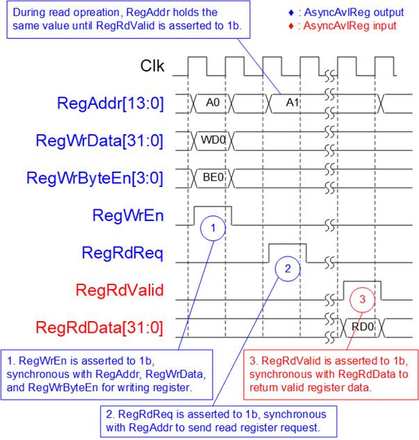
Figure 12 Register Interface Timing Diagram
1) Timing diagram to write register is similar to that of a single-port RAM. The RegWrEn signal is set to 1b, along with a valid RegAddr (Register address in 32-bit units), RegWrData (write data for the register), and RegWrByteEn (write byte enable). The byte enable consists of four bits that indicate the validity of the byte data. For example, bit[0], [1], [2], and [3] are set to 1b when RegWrData[7:0], [15:8], [23:16], and [31:24] are valid, respectively.
3) The slave returns the read data on RegRdData bus by setting the RegRdValid signal to 1b. After that, AsyncAvlReg forwards the read value to the SAvlRead interface.
2.3.2 UserReg
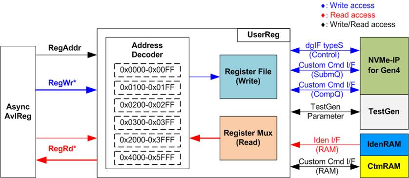
Figure 13 UserReg Interface
· 0x0000 – 0x00FF: Mapped to set the command with the parameters of NVMe-IP and TestGen.
· 0x0100 – 0x01FF: Mapped to status registers of NVMe-IP and TestGen. This region supports read-access only.
· 0x0200 – 0x02FF: Mapped to set the parameters for Custom command interface of NVMe-IP.
· 0x0300 – 0x03FF: Mapped to status registers of the Custom command interface of NVMe-IP. This region supports read-access only.
· 0x2000 – 0x3FFF: Mapped to IdenRAM, used for reading Identify command data. This region is read-access only.
· 0x4000 – 0x5FFF: Mapped to the Custom Command RAM Interface. While this interface supports both read and write operations, the demo design utilizes read access only when executing the SMART command.
The Address decoder decodes the upper bits of RegAddr to select the appropriate hardware module (NVMe-IP, TestGen, IdenRAM, or CtmRAM). The Register File within the UserReg module operates on a 32-bit bus size, so the write byte enable (RegWrByteEn) is not used in the test system. The CPU interacts with the hardware registers using 32-bit aligned pointers.
For read operations, multi-level multiplexers (mux) are used to select the correct data to return to the CPU based on the input address. The lower bits of RegAddr are passed to the respective submodules to select specific register values, while the upper bits are used within UserReg to determine which submodule’s data is selected.
As a result, the read data latency is three clock cycles. The signal “RegRdValid” is generated by delaying “RegRdReq”, through three D Flip-flops, ensuring proper timing and synchronization. Additional details on the address mapping within the UserReg module are provided in Table 1.
Table 1 Register Map
|
Address |
Register Name |
Description |
|
Wr/Rd |
(Label in “nvmeiptest_ag5.c”) |
|
|
0x0000 – 0x00FF: Control Signals of NVMe-IP and TestGen |
||
|
BA+0x0000 |
User Address (Low) Reg |
[31:0]: Input to be bits[31:0] of start address as 512-byte units (UserAddr[31:0] of dgIF typeS) |
|
Wr/Rd |
(USRADRL_INTREG) |
|
|
BA+0x0004 |
User Address (High) Reg |
[15:0]: Input to be bits[47:32] of start address as 512-byte units (UserAddr[47:32] of dgIF typeS) |
|
Wr/Rd |
(USRADRH_INTREG) |
|
|
BA+0x0008 |
User Length (Low) Reg |
[31:0]: Input to be bits[31:0] of transfer length as 512-byte units (UserLen[31:0] of dgIF typeS) |
|
Wr/Rd |
(USRLENL_INTREG) |
|
|
BA+0x000C |
User Length (High) Reg |
[15:0]: Input to be bits[47:32] of transfer length as 512-byte units (UserLen[47:32] of dgIF typeS) |
|
Wr/Rd |
(USRLENH_INTREG) |
|
|
BA+0x0010 |
User Command Reg |
[2:0]: Input to be user command (UserCmd of dgIF typeS for NVMe-IP) 000b: Identify, 001b: Shutdown, 010b: Write SSD, 011b: Read SSD, 100b: SMART/Secure Erase, 110b: Flush, 101b/111b: Reserved Writing to this register triggers the command request to NVMe-IP to start the operation. |
|
Wr/Rd |
(USRCMD_INTREG) |
|
|
BA+0x0014 |
Test Pattern Reg |
[2:0]: Select test pattern 000b-Increment, 001b-Decrement, 010b-All 0, 011b-All 1, 100b-LFSR |
|
Wr/Rd |
(PATTSEL_INTREG) |
|
|
BA+0x0020 |
NVMe Timeout Reg |
[31:0]: Mapped to TimeOutSet[31:0] of NVMe-IP |
|
Wr/Rd |
(NVMTIMEOUT_INTREG) |
|
|
0x0100 – 0x01FF: Control Signals of NVMe-IP and TestGen (Read-Access Only) |
||
|
BA+0x0100 |
User Status Reg |
[0]: UserBusy of dgIF typeS (0b: Idle, 1b: Busy) [1]: UserError of dgIF typeS (0b: Normal, 1b: Error) [2]: Data verification fails (0b: Normal, 1b: Error) |
|
(USRSTS_INTREG) |
||
|
BA+0x0104 |
Total disk size (Low) Reg |
[31:0]: Mapped to LBASize[31:0] of NVMe-IP |
|
(LBASIZEL_INTREG) |
||
|
BA+0x0108 |
Total disk size (High) Reg |
[15:0]: Mapped to LBASize[47:32] of NVMe-IP [31]: Mapped to LBAMode of NVMe-IP |
|
(LBASIZEH_INTREG) |
||
|
BA+0x010C |
User Error Type Reg |
[31:0]: Mapped to UserErrorType[31:0] of NVMe-IP to show error status |
|
(USRERRTYPE_INTREG) |
||
|
BA+0x0110 |
PCIe Status Reg |
[0]: PCIe linkup status from PCIe Hard IP (0b: No linkup, 1b: linkup) [3:2]: Two lower bits to show PCIe link speed from PCIe Hard IP. The upper bit is located at bit[16]. (000b: Not linkup, 001b: PCIe Gen1, 010b: PCIe Gen2, 011b: PCIe Gen3, 111b: PCIe Gen4) [6:4]: PCIe link width status from PCIe Hard IP (001b: 1-lane, 010b: 2-lane, 100b: 4-lane) [13:8]: Current LTSSM State of PCIe Hard IP. Please see more details of LTSSM value in PCIe Hard IP datasheet. [16]: The upper bit to show PCIe link speed of PCIe Hard IP. The lower two bits are located at bits[3:2]. |
|
(PCIESTS_INTREG) |
||
|
BA+0x0114 |
Completion Status Reg |
[15:0]: Mapped to AdmCompStatus[15:0] of NVMe-IP [31:16]: Mapped to IOCompStatus[15:0] of NVMe-IP |
|
(COMPSTS_INTREG) |
||
|
BA+0x0118 |
NVMe CAP Reg |
[31:0]: Mapped to NVMeCAPReg[31:0] of NVMe-IP |
|
(NVMCAP_INTREG) |
||
|
BA+0x011C |
NVMe IP Test Pin Reg |
[31:0]: Mapped to TestPin[31:0] of NVMe-IP |
|
(NVMTESTPIN_INTREG) |
||
|
Address |
Register Name |
Description |
|
Wr/Rd |
(Label in “nvmeiptest_ag5.c”) |
|
|
0x0100 – 0x01FF: Control Signals of NVMe-IP and TestGen (Read-Access Only) |
||
|
BA+0x0130 - BA+0x014F |
Expected Value Word0-7 Reg |
256-bit expected data at the 1st failure data when executing a Read command. 0x0130: Bits[31:0], 0x0134: Bits[63:32], …, 0x014C: Bits[255:224] |
|
(EXPPATW0-W7_INTREG) |
||
|
BA+0x0150 - BA +0x016F |
Read value Word0-7 Reg |
256-bit read data of the 1st failure when executing a Read command. 0x0150: Bits[31:0], 0x0154: Bits[63:32], …, 0x016C: Bits[255:224] |
|
(RDPATW0-W7_INTREG) |
||
|
BA+0x0170 |
Data Failure Address(Low) Reg |
[31:0]: Bits[31:0] of the byte address of the 1st failure when executing a Read command |
|
(RDFAILNOL_INTREG) |
||
|
BA+0x0174 |
Data Failure Address(High) Reg |
[24:0]: Bits[56:32] of the byte address of the 1st failure when executing a Read command |
|
(RDFAILNOH_INTREG) |
||
|
BA+0x0178 |
Current Test Byte (Low) Reg |
[31:0]: Bits[31:0] of the current test data size in the TestGen module |
|
(CURTESTSIZEL_INTREG) |
||
|
BA+0x017C |
Current Test Byte (High) Reg |
[24:0]: Bits[56:32] of the current test data size in the TestGen module |
|
(CURTESTSIZEH_INTREG) |
||
|
Other Interfaces (Custom Command of NVMe-IP, IdenRAM, and Custom RAM) |
||
|
BA+0x0200 - BA+0x023F |
Custom Submission Queue Reg |
[31:0]: Submission queue entry for SMART, Secure Erase, and Flush commands. Input to be CtmSubmDW0-DW15 of NVMe-IP 0x0200: DW0, 0x0204: DW1, …, 0x023C: DW15 |
|
Wr/Rd |
(CTMSUBMQ_STRUCT) |
|
|
BA+0x0300 - BA+0x030F |
Custom Completion Queue Reg |
[31:0]: CtmCompDW0-DW3 output from NVMe-IP 0x0300: DW0, 0x0304: DW1, …, 0x030C: DW3 |
|
Rd |
(CTMCOMPQ_STRUCT) |
|
|
BA+0x0800 |
IP Version Reg |
[31:0]: Mapped to IPVersion[31:0] of NVMe-IP |
|
Rd |
(IPVERSION_INTREG) |
|
|
BA+0x2000 - BA+0x2FFF |
Identify Controller Data |
4KB Identify Controller Data structure. |
|
Rd |
(IDENCTRL_CHARREG) |
|
|
BA+0x3000 - BA+0x3FFF |
Identify Namespace Data |
4KB Identify Namespace Data structure. |
|
Rd |
(IDENNAME_CHARREG) |
|
|
BA+0x4000 - BA+0x5FFF |
Custom Command RAM |
Connect to the 8KB CtmRAM interface for storing 512-byte data output from the SMART command. |
|
Wr/Rd |
(CTMRAM_CHARREG) |
|
3 CPU Firmware
3.1 Test Firmware (nvmeiptest_ag5.c)
Upon system startup, the CPU follows these steps to complete the initialization process.
1) Initialize the JTAG UART and Timer settings.
2) Wait for the PCIe connection to become active by checking if PCIESTS_INTREG[0]=1b.
3) Wait for NVMe-IP to complete its own initialization process by monitoring USRSTS_INTREG[0]=0b. If an error is encountered, the process will terminate and display an error message.
4) Display the status of the PCIe link, including the number of lanes and the speed, by reading PCIESTS_INTREG[16:2].
5) Display the main menu, providing options to execute seven NVMe-IP commands: Identify, Write, Read, SMART, Flush, Secure Erase, and Shutdown.
Details of each command sequence in the CPU firmware are described in the following sections.
3.1.1 Identify Command
When the user selects the Identify command, the firmware executes the following sequence.
1) Set bits[2:0] of USRCMD_INTREG to 000b to send the Identify command request to NVMe-IP. The busy flag (USRSTS_INTREG[0]) then changes from 0b to 1b.
2) The CPU monitors USRSTS_INTREG[1:0] to determine whether the operation completes or an error occurs.
· Bit[0] is de-asserted to 0b when the command is completed. The Identify command data returned by NVMe-IP is stored in IdenRAM.
· Bit[1] is asserted to 1b, indicating an error. In this case, the CPU displays an error message on the console with details decoded from USRERRTYPE_INTREG[31:0]. The process will then be terminated.
3) Once the busy flag (USRSTS_INTREG[0]) is de-asserted to 0b, the CPU proceeds to display information that has been decoded from LBASIZEL/H_INTREG, which includes the SSD capacity and LBA unit size. In addition, further information, such as the SSD model, can be retrieved from the IdenRAM (IDENCTRL_CHARREG).
3.1.2 Write/Read Command
When the Write/Read command is selected, the firmware follows this sequence.
1) The CPU receives the start address, transfer length, and test pattern from the console. If any inputs are invalid, the operation will be cancelled.
Note: If LBA unit size is 4 KB, the start address and transfer length must align to 8.
2) Once all inputs are validated, the values are written to USRADRL/H_INTREG, USRLENL/H_INTREG, and PATTSEL_INTREG.
3) To execute a Write command, set bits[2:0] of USRCMD_INTREG to 010b, or for a Read command, set it to 011b. This sends the command request to the NVMe-IP. Once the command is issued, the busy flag of NVMe-IP (USRSTS_INTREG[0]) will change from 0b to 1b.
4) The CPU waits until the operation is completed or an error (excluding verification error) is detected by monitoring USRSTS_INTREG[2:0].
· Bit[0] is de-asserted to 0b when the command is completed.
· Bit[1] is asserted to 1b, indicating an error. An error message is displayed on the console with details from USRERRTYPE_INTREG[31:0], and the process will then be terminated.
· Bit[2] is asserted when data verification fails. The verification error message is displayed on the console, but the CPU will continue running until the operation is completed.
While the command is running, the current transfer size is read from CURTESTSIZEL/H_INTREG and displayed every second.
5)
Once the busy flag (USRSTS_INTREG[0])
is de-asserted to 0b, the CPU calculates and displays the test result on the
console, including the total time usage, total transfer size, and transfer
speed.
3.1.3 SMART Command
When the SMART command is selected, the firmware follows this sequence.
1) The CPU configures the 16 Dwords of the Submission Queue entry (CTMSUBMQ_STRUCT) with the SMART command value.
2) Set bits[2:0] of USRCMD_INTREG[2:0] to 100b to send the SMART command request to NVMe-IP. The busy flag (USRSTS_INTREG[0]) then changes from 0b to 1b.
3) The CPU waits until the operation is completed or an error is detected by monitoring USRSTS_INTREG[1:0].
· Bit[0] is de-asserted to 0b after the operation is finished. The SMART command data returned by NVMe-IP is stored in CtmRAM.
· Bit[1] is asserted to 1b, indicating an error. An error message is displayed on the console with details from USRERRTYPE_INTREG[31:0]. The process will then be terminated.
4) Once the busy flag (USRSTS_INTREG[0]) is de-asserted to 0b, the CPU retrieves and displays SMART information decoded from CtmRAM (CTMRAM_CHARREG), including Remaining Life, Percentage Used, Temperature, Total Data Read, Total Data Written, Power-On Cycles, Power-On Hours, and Number of Unsafe Shutdown.
For more details on the SMART log, refer to the NVM Express Specification.
https://nvmexpress.org/specifications/
3.1.4 Flush Command
When the user selects the Flush command, the firmware follows this sequence.
1) The 16 Dwords of the Submission Queue entry (CTMSUBMQ_STRUCT) are configured with the Flush command value.
2) Set bits[2:0] of USRCMD_INTREG[2:0] to 110b to send Flush command request to NVMe-IP. The busy flag of NVMe-IP (USRSTS_INTREG[0]) then changes from 0b to 1b.
3) The CPU waits until the operation is completed or an error is detected by monitoring USRSTS_INTREG[1:0].
· Bit[0] is de-asserted to 0b after the operation is finished. The CPU will then return to the main menu.
· Bit[1] is asserted to 1b, indicating an error. An error message is displayed on the console with details from USRERRTYPE_INTREG[31:0]. The process will then be terminated.
3.1.5 Secure Erase Command
When the user selects the Secure Erase command, the firmware follows this sequence.
1) The 16 Dwords of the Submission Queue entry (CTMSUBMQ_STRUCT) are configured with the Secure Erase command value.
2) Set NVMTIMEOUT_INTREG to 0 to disable the timer and prevent a timeout error during the operation.
3) Set bits[2:0] of USRCMD_INTREG[2:0] to 100b to send Secure Erase command request to NVMe-IP. The busy flag of NVMe-IP (USRSTS_INTREG[0]) changes from 0b to 1b.
4) The CPU waits until the operation is completed or an error is detected by monitoring USRSTS_INTREG[1:0].
· Bit[0] is de-asserted to 0b after the operation is finished. The CPU proceeds to the next step.
· Bit[1] is asserted to 1b, indicating an error. An error message is displayed on the console with details from USRERRTYPE_INTREG[31:0]. The process will then be terminated.
5) Once the command completes, the timer is re-enabled by restoring NVMTIMEOUT_INTREG to its default value, allowing timeout error to be detected by NVMe-IP. The CPU then returns to the main menu.
3.1.6 Shutdown Command
When the Shutdown command is selected, the firmware follows this sequence.
1) Set bits[2:0] of USRCMD_INTREG to 001b to send the Shutdown command request to NVMe-IP. The busy flag of NVMe-IP (USRSTS_INTREG[0]) then changes from 0b to 1b.
2) The CPU waits until the operation is completed or an error is detected by monitoring USRSTS_INTREG[1:0].
· Bit[0] is de-asserted to 0b after the operation is completed. The CPU proceeds to the next step.
· Bit[1] is asserted to 1b, indicating an error. An error message is displayed on the console with details from USRERRTYPE_INTREG[31:0]. The process will then be terminated.
3) After the Shutdown command completes, both the SSD and NVMe-IP become inactive, and the CPU no longer accepts new commands from the user. To resume testing, the user must power off and subsequently power on the system.
3.2 Function List in Test Firmware
This section describes the list of functions used to operate NVMe-IP for Gen4.
|
void error_handler(void) |
|
|
Parameters |
None |
|
Return value |
None |
|
Description |
Invoked when an error occurs in the system. The default behavior is to enter an infinite loop, effectively halting all further operation. This function can be customized by the user to implement specific error recovery procedures, such as resetting the system or logging diagnostics. |
|
int exec_ctm(unsigned int user_cmd) |
|
|
Parameters |
user_cmd: Command type (4-SMART/Secure Erase command, 6-Flush command) |
|
Return value |
STATUS_SUCCESS: Command execution completed successfully STATUS_ERROR: Error occurred during the operation |
|
Description |
Execute SMART command as outlined in Section 3.1.3 (SMART Command), execute Flush command as outlined in Section 3.1.4 (Flush Command), or execute Secure Erase command as outlined in Section 3.1.5 (Secure Erase Command). |
|
void get_cursize(unsigned long long* cursize) |
|
|
Parameters |
cursize: A pointer to store the current transfer size (bytes) |
|
Return value |
None |
|
Description |
Read the current transfer size from CURTESTSIZEL/H_INTREG. Combines the two 32-bit register values into a 64-bit number and stores the result in the memory location pointed to by ‘cursize’. |
|
int get_param(userin_struct* userin) |
|
|
Parameters |
userin: Pointer to user input structure for capturing parameters (start address, total length in 512-byte units, and test pattern) |
|
Return value |
STATUS_SUCCESS: All inputs are valid and successfully stored. STATUS_INVALIDINPUT: One or more inputs are invalid. |
|
Description |
Receive and validate user input. If the input is invalid, the function returns ‘STATUS_INVALIDINPUT’. Otherwise, the inputs are updated in the userin structure. |
|
int iden_dev(void) |
|
|
Parameters |
None |
|
Return value |
STATUS_SUCCESS: Operation completed successfully STATUS_ERROR: Error occurred during execution |
|
Description |
Execute Identify command as outlined in Section 3.1.1 (Identify Command). |
|
int setctm_erase(void) |
|
|
Parameters |
None |
|
Return value |
STATUS_SUCCESS: Operation completed successfully STATUS_ERROR: Error occurred during execution STATUS_CANCEL: Operation is cancelled |
|
Description |
Set Secure Erase command to ‘CTMSUBMQ_STRUCT’ and call ‘exec_ctm’ function to execute Secure Erase command. |
|
int setctm_flush(void) |
|
|
Parameters |
None |
|
Return value |
STATUS_SUCCESS: Operation completed successfully STATUS_ERROR: Error occurred during execution |
|
Description |
Set Flush command to ‘CTMSUBMQ_STRUCT’ and call ‘exec_ctm’ function to execute Flush command. |
|
int setctm_smart(void) |
|
|
Parameters |
None |
|
Return value |
STATUS_SUCCESS: Operation completed successfully STATUS_ERROR: Error occurred during execution |
|
Description |
Set SMART command to ‘CTMSUBMQ_STRUCT’ and call ‘exec_ctm’ function to execute SMART command. Finally, decode and display SMART information on the console. |
|
void show_error(void) |
|
|
Parameters |
None |
|
Return value |
None |
|
Description |
Reads the error type from ‘USRERRTYPE_INTREG’, decodes detailed error categories, and displays them on the console. Also, call ‘show_pciestat’ function to display internal debug values. |
|
void show_pciestat(void) |
|
|
Parameters |
None |
|
Return value |
None |
|
Description |
Read ‘PCIESTS_INTREG’ and display its value on the console. Also, read and display debug signals from ‘NVMTESTPIN_INTREG’. |
|
void show_result(void) |
|
|
Parameters |
None |
|
Return value |
None |
|
Description |
Execute the following steps. 1) Update the total transfer size by calling ‘get_cursize’ function and display the result on the console using the ‘show_size’ function. 2) Display the total time. 3) Calculate and display the transfer performance. |
|
void show_size(unsigned long long size_input) |
|
|
Parameters |
size_input: Transfer size in bytes |
|
Return value |
None |
|
Description |
Calculate and display the ‘size_input’ value in MB or GB units on the console. |
|
void show_smart_hex16byte(volatile unsigned char *char_ptr) |
|
|
Parameters |
*char_ptr: Pointer of 16-byte SMART data block |
|
Return value |
None |
|
Description |
Display a 16-byte SMART data block as a hexadecimal string on the console. |
|
void show_smart_int8byte(volatile unsigned char *char_ptr) |
|
|
Parameters |
*char_ptr: Pointer of 8-byte SMART data block |
|
Return value |
None |
|
Description |
Display 8-byte SMART data in decimal units if the input value is less than 4 billion (32-bit). Otherwise, an overflow message is displayed. |
|
void show_smart_size8byte(volatile unsigned char *char_ptr) |
|
|
Parameters |
*char_ptr: Pointer of 8-byte SMART data block |
|
Return value |
None |
|
Description |
Display 8-byte SMART data in GB or TB units. If the input value exceeds 500 PB, an overflow message is displayed. |
|
void show_vererr(void) |
|
|
Parameters |
None |
|
Return value |
None |
|
Description |
Read the first failing byte address from ‘RDFAILNOL/H_INTREG’, the expected data from ‘EXPPATW0-W7_INTREG’, and the read value from ‘RDPATW0-W7_INTREG’. These details are displayed on the console to provide information on verification errors. |
|
int shutdown_dev(void) |
|
|
Parameters |
None |
|
Return value |
STATUS_SUCCESS: Operation completed successfully STATUS_ERROR: Error occurred during execution |
|
Description |
Execute the Shutdown command as outlined in Section 3.1.6 (Shutdown Command). |
|
int wrrd_dev(unsigned int user_cmd) |
|
|
Parameters |
user_cmd: Operation type (2-Write command, 3-Read command) |
|
Return value |
STATUS_SUCCESS: Operation completed successfully STATUS_ERROR: Error occurred during execution STATUS_INVALIDINPUT: User input is invalid or out of range |
|
Description |
Execute Write command and Read command as outlined in Section 3.1.2 (Write/Read Command). Call ‘show_result’ function to calculate and display transfer performance for the Write and Read commands. |
4 Example Test Result
The demo system was tested using a 6.4 TB MEMBLAZE P7A46DT0640Y00 SSD on Atum A5 Development Kit. The results of the tests are presented in Figure 14. The system’s performance was measured using the Write and Read commands, with the test data pattern set to LFSR and a transfer size of 64 GB.
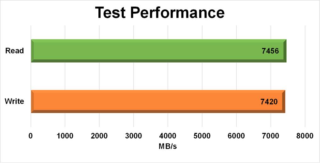
Figure 14 Test Performance of Write and Read Commands
The Atum A5 Development Kit with PCIe Gen4 delivers impressive PCIe Gen4 storage performance, achieving approximately 7420 MB/s write and 7456 MB/s read throughput.
5 Revision History
|
Revision |
Date (D-M-Y) |
Description |
|
1.00 |
13-Jul-26 |
Initial version release |