NVMeG4-IP with DMA on PetaLinux
Reference Design Manual
1 Overview

Figure 1 Comparison of NVMe Solutions on PetaLinux Using Zynq UltraScale+
On Zynq UltraScale+ evaluation boards, such as the AMD ZCU106, which integrates a PCIe Gen3 Hard IP block, the conventional solution for accessing an NVMe Gen3 SSD is illustrated on the left side of Figure 1. This approach typically uses the XDMA IP Core as the PCIe interface, combined with a standard NVMe device driver running on PetaLinux OS. When using standard benchmark tools such as “dd” and “fio”, this setup achieves a transfer performance of approximately 2000 MB/s, or about 57% of 3500 MB/s maximum performance of NVMe Gen3 SSD.
In contrast, Design Gateway solution, shown on the right side of Figure 1, does not require a PCIe Hard IP. Instead, it relies solely on transceivers that support PCIe Gen4 speed. This enables evaluation boards like the AMD ZCU102 and ZCU106 to interface with an NVMe Gen4 SSD, achieving data transfer rates of approximately 7000 MB/s. The DG solution includes the NVMeG4 IP core, which combines an NVMe protocol handler with a PCIe Soft IP and connects to the SSD through the PCIe PHY IP. An AXI DMA IP core is also integrated to handle high-speed data transfers between the NVMeG4-IP and the host memory for CPU access.
To support this architecture on PetaLinux OS, the DG NVMe Driver is developed specifically too interface with NVMeG4-IP. Since NVMeG4-IP is a fully offloaded engine for handling NVMe operations, much of the protocol handling normally managed by a standard NVMe software driver is offloaded to hardware. As a result, the system requires significantly less CPU resource – limited mainly to parameter configuration and status monitoring during test application execution. Ultimately, this hardware-accelerated solution enables the demo to achieve full throughput performance of 7000 MB/s for both write and read operations to the NVMe Gen4 SSD.
2 Hardware
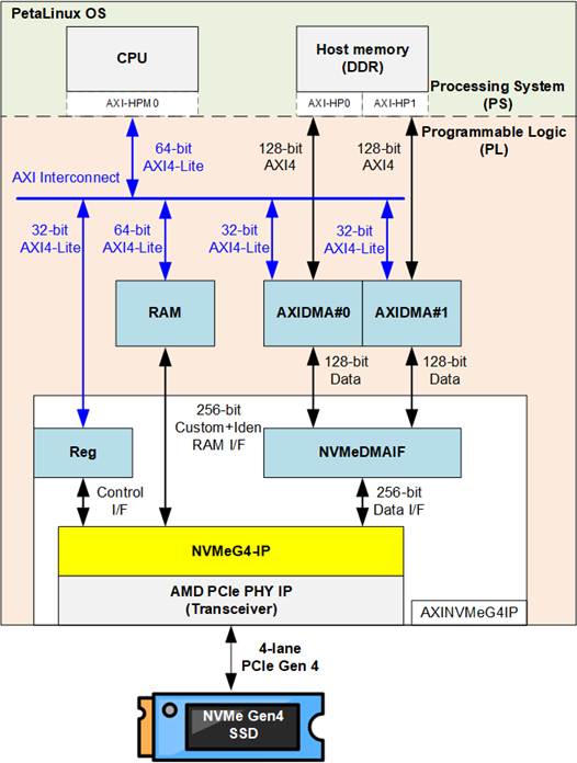
Figure 2 Hardware System for NVMeG4-IP with DMA on PetaLinux Demo
To implement the hardware accelerator in the Programmable Logic (PL) for cooperation with the Processing System (PS), two standard AXI bus interfaces are used: AXI4-Lite for low-speed control and AXI4 for high-speed data transfer with host memory. Since the maximum data width of AXI High-Performance (AXI-HP) interface is 128 bits, which is a half the data width of the NVMeG4-IP, two AXI-HP interfaces are used to support full-bandwidth data transfer - approximately 7000 MB/s, the performance of an NVMe Gen4 SSD.
The user interface of NVMeG4-IP is divided into three functional groups: the Control I/F, the Custom-Identify RAM I/F, and the Data I/F. The Control I/F is responsible for issuing commands, setting parameters, and monitoring the status of the IP core. The Control I/F is mapped to a Register module, which connects to the CPU through AXI-HPM interface. When executing SMART and Identify commands, the NVMeG4-IP retrieves 512-byte and 8 KB data blocks, respectively, from the SSD and uploads them to internal RAM. The CPU then accesses this information through the AXI-HPM interface, which is suited for low-speed control and status transactions.
For high-speed operations (the write and read commands), efficient data movement between the PL and the host memory is essential. To facilitate this, the design integrates AMD AXI DMA IP core, which enables direct data transfers between the NVMeG4-IP and host memory without heavy CPU involvement. AMD also provides a dedicated device driver for this IP core, allowing application-level access to hardware buffers through standard software interfaces.
Since the NVMeG4-IP operates with a 256-bit data width – double that of a single DMA channel (128 bits) – the design utilizes two AXI DMA modules in parallel to handle full-bandwidth data transfer. To manage and coordinate the data flow between these DMA modules and the NVMeG4-IP, a dedicated component called the NVMeDMAIF is implemented. This adapter ensures proper block-based data transfer, maintaining high throughput across the entire transfer path. Additionally, both AXI DMA IPs are controlled by the CPU via AXI4-Lite bus.
This section focuses on the hardware components implemented in the PL. The following section (Section 3) will describe the corresponding software components designed to run on PetaLinux OS.
2.1 AXINVMeG4IP
This module encapsulates the customized hardware components, including the NVMeG4-IP, and is exported as an IP Integrator block for integration with other AMD IP cores within the Vivado Block Design environment. Figure 3 illustrates the internal structure and submodules of the AXINVMeG4IP.
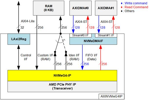
Figure 3 AXINVMeG4IP Block Diagram
The AXINVMeG4IP module functions as a bridge, enabling integration of the NVMeG4-IP into the overall system. All user interfaces of the NVMeG4-IP are converted into standard interfaces through supporting submodules. The LAxi2Reg module handles the control and status signals of the NVMeG4-IP by implementing a register map accessible through a 32-bit AXI4-Lite bus for communication with the processor.
An 8 KB RAM is included to store the retrieved data from the SMART command (via the Custom I/F) and the Identify command (via the Iden I/F). Simple control logic is used to select the appropriate interface when writing to the RAM. In addition, NVMeG4-IP features a data input path mapped from the same RAM to support future commands that require input data.
For high-speed data transfer, the NVMeDMAIF includes internal buffering to manage data streams between two 128-bit AXI4-Stream (AXI4-ST) interfaces and a 256-bit FIFO interface. This mechanism ensures efficient handling of write and read operations with proper data alignment and throughput.
Further details of each submodule are provided in the following sections.
2.1.1 NVMeDMAIF
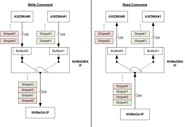
Figure 4 Data Block Handler of NVMeDMAIF
The NVMeDMAIF is designed to manage high-speed data streaming between two 128-bit data interface of the AXI DMA IPs and the 256-bit data interface of the NVMeG4-IP. To facilitate this, the adapter incorporates two internal buffers that serve both as temporary data storage and as a bridge for data width conversion between the 128-bit and 256-bit buses.
Each buffer is segmented into units called “stripe sizes” to enable efficient data interleaving. As illustrated in Figure 4, during write command execution, the data source alternates between Buffer#0 and Buffer#1 upon completion of each stripe transfer. This interleaving behavior emulates a RAID0 (striping) configuration, enabling parallelism and maximizing throughput from both AXI DMA engines.
Similarly, during read command execution, data received from the NVMeG4-IP is alternately written to Buffer#0 and Buffer#1, switching destinations after each stripe. This approach maintains the same RAID0-style behavior, ensuring balanced bandwidth utilization and efficient parallel data handling.
In this reference design, the stripe size is fixed at 4 KB, aligning with the default memory page size used by the PetaLinux OS.
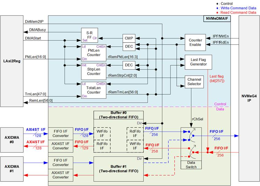
Figure 5 NVMeDMAIF Hardware
Figure 5 illustrates two component groups of the NVMeDMAIF architecture: the upper section, which contains the control logic responsible for managing data flow, and the lower section, which represents the data transfer path between the AXI DMA modules and the NVMeG4-IP.
In the upper section, the operation begins when a new command request is received from the LAxi2Reg module. At this point, the NVMeDMAIF determines the direction of data transfer using the “DirMem2IP” signal. A value of 1b indicates that data will be transferred from the AXI DMA to the NVMeG4-IP (write command), whereas a value of 0b designates a transfer from the NVMeG5-IP to the AXI DMA (read command).
Three counters are used to manage and coordinate the data transfer process. The first, called the PktLen counter, functions as a down-counter that segments the incoming data stream from the NVMeG4-IP into packets. When the counter reaches threshold, it triggers the assertion of the last flag along with the final packet data, signaling that the current packet is complete.
The second counter, the StrpLen counter, is also a down-counter and is used to implement data striping between the two DMA channels. With a fixed stripe size of 4 KB, this counter decrements with each transfer. When its value reaches threshold, it toggles the rChSel signal. This action alternates the active buffer between Buffer#0 and Buffer#1, enabling efficient interleaving of data streams and emulating a RAID0-style configuration.
The final counter is the TotalLen counter, which tracks the entire length of the data transfer. When this counter reaches threshold, the DMABusy signal is de-asserted, indicating that the transfer has completed. In read operations, when the TotalLen counter finishes counting down, the last flag is also asserted to mark the conclusion of the final data packet.
The lower section of Figure 5 depicts the data path architecture of NVMeDMAIF, which handles bidirectional transfer operations – Write and Read. During execution of the Write command, data originates from the AXI DMA modules and is transmitted through 128-bit AXI4-Stream (AXI4-ST) interfaces. This data is first processed by FIFO I/F converters, which transform the AXI4-ST format into a compatible FIFO interface for the Buffer.
Following this conversion, the data is written into dedicated buffer structures implemented as two-directional FIFOs. Each two-directional FIFO is constructed using a 16 KB true dual-port RAM and additional adapter logic that transforms the RAM’s native interface into FIFO-compatible read/write access. Since Write and Read commands are never active at the same time, the same dual-port RAM can be reused for both directions, optimizing resource usage.
To accommodate the two AXI DMA channels, the system uses two identical sets of FIFO I/F converters and two-directional FIFOs—one set for each DMA input. After data is written into the buffers, the Data Switch module takes over to manage read access to the NVMeG4-IP. It selects which buffer to forward data from, alternating every 4 KB of data to implement a striping pattern that represents RAID0 behavior. This interleaved output is then transmitted to the NVMeG4-IP at its 256-bit data interface for final storage on the SSD.
During the execution of the Read command, the NVMeG4-IP transmits a 256-bit data stream over a FIFO interface. This output data, including a last flag to indicate the end of each packet, is directed into one of the two two-directional FIFOs. The buffer selection is managed by the rChSel signal, which toggles after every completed stripe transfer (fixed at 4 KB) to enable alternating data storage between Buffer#0 and Buffer#1.
Once stored, the buffered data is retrieved and forwarded to the AXI DMA modules. This is achieved through the AXI4ST I/F Converter, which converts the FIFO-format 256-bit data back into the 128-bit AXI4-ST format compatible with the AXI DMA IPs.
2.1.2 NVMeG4-IP
The NVMeG4-IP implements NVMe protocol of the host side to direct access an NVMe Gen4 SSD without PCIe switch connection. Besides, it includes PCIe soft IP operating with PCIe PHY to support the same feature as PCIe hard IP. It supports seven commands, i.e., Write, Read, Identify, Shutdown, SMART, Secure Erase, and Flush. More details of NVMeG4-IP are described in datasheet.
https://dgway.com/products/IP/NVMe-IP/dg_nvmeg4_ip_data_sheet_xilinx_en/
2.1.3 AMD PCIe PHY
The PCIe PHY is provided by AMD to enable the utilization of Soft IP instead of Hard IP to construct a PCIe MAC. The PCIe PHY utilizes the PHY Interface for PCIe Express (PIPE) as its user interface. To operate with the NVMeG4-IP, it is configured to 4-lane, with each lane operating at 16.0 GT/s. For more detailed information of the PCIe PHY, please refer to the “PG239: PCI Express PHY” document, available at AMD website
https://docs.amd.com/r/en-US/pg239-pcie-phy
2.1.4 LAxi2Reg
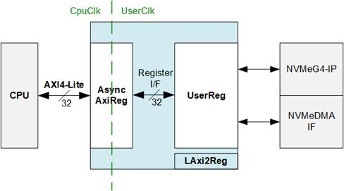
Figure 6 LAxi2Reg Block Diagram
The LAxi2Reg submodule serves as the control interface between the CPU and the hardware modules, including the NVMeG4-IP and the NVMeDMAIF. It manages register access and configuration via two main submodules: AsyncAxiReg and UserReg.
The CPU communicates with the LAxi2Reg module over a 32-bit AXI4-Lite interface. Incoming register accesses are initially handled by the AsyncAxiReg submodule, which converts AXI4-Lite protocol signals into a simplified Register interface with a 32-bit data bus size, matching the width of the AXI4-Lite interface. This submodule also incorporates asynchronous logic to safely manage clock domain crossing between the CpuClk and UserClk domains.
Once synchronization is complete, register write and read operations are passed to the UserReg submodule. This block implements the user-defined control and status registers that directly drive the internal control signals of both the NVMeG4IP core and the NVMeDMAIF.
AsyncAxiReg
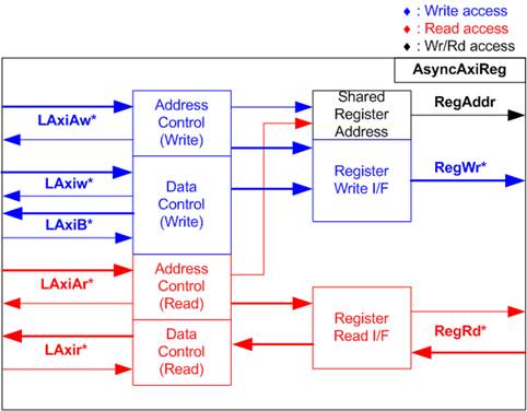
Figure 7 AsyncAxiReg Interface
The signals on AXI4-Lite bus interface are divided into five groups: LAxiAw* (Write address channel), LAxiw* (Write data channel), LAxiB* (Write response channel), LAxiAr* (Read address channel), and LAxir* (Read data channel). For more information on designing custom logic for the AXI4-Lite bus, refer to the following documentation.
In accordance with the AXI4-Lite standard, the write and read channels operate independently, with separate control and data interfaces for each channel. Therefore, the logic inside AsyncAxiReg that interfaces with the AXI4-Lite bus is divided into four functional groups: Write control logic, Write data logic, Read control logic, and Read data logic, as depicted on the left side of Figure 7. The Write control I/F and Write data I/F of the AXI4-Lite bus are latched and then transferred to the Write register interface via clock domain crossing registers. Similarly, the Read control I/F of the AXI4-Lite bus is latched and transferred to the Read register interface. The data returned from the Register Read I/F is transferred back to the AXI4-Lite bus by using clock domain crossing registers. In the Register interface, RegAddr is shared between write and read access, so the address is loaded from LAxiAw for write access or from LAxiAr for read access.
The simple register interface is designed to be compatible with a single-port RAM interface for write transaction. For read transaction, the Register interface is slightly modified from the RAM interface by adding RdReq and RdValid signals to control read latency. Since the address of the Register interface is shared for both write and read transactions, the user cannot perform simultaneous write and read operations. The timing diagram for the Register interface is shown in Figure 8.
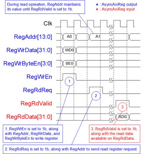
Figure 8 Register Interface Timing Diagram
1) Timing diagram to write register is similar to that of a single-port RAM. The RegWrEn signal is set to 1b, along with a valid RegAddr (Register address in 32-bit units), RegWrData (write data for the register), and RegWrByteEn (write byte enable). The byte enable is four bits wide, where each bit indicates the validity of a specific byte within RegWrData. For example, if RegWrByteEn[0], [1], [2], and [3] are set to 1b, then RegWrData[7:0], [15:8], [23:16], and [31:24] are valid, respectively.
2) To read from a register, AsyncAxiReg sets the RegRdReq signal to 1b, along with a valid value for RegAddr. After the read request is processed, the 32-bit data is returned. The slave detects the RegRdReq being asserted to start the read transaction. During the read operation, the address value (RegAddr) remains unchanged until RegRdValid is set to 1b. Once valid, the address is used to select the returned data through multiple layers of multiplexers.
3) The slave returns the read data on RegRdData bus by setting the RegRdValid signal to 1b. After that, AsyncAxiReg forwards the read value to the LAxir* interface.
UserReg
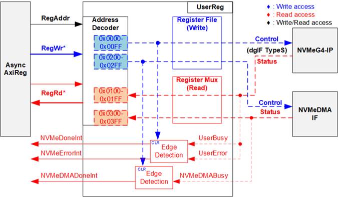
Figure 9 UserReg Interface
The UserReg module consists of three main components: an Address Decoder, a Register File, and a Register Mux. The Address Decoder interprets the address received from AsyncAxiReg submodule to select the appropriate register for either write or read operations. The address space managed by UserReg is divided into two regions, as illustrated in Figure 9:
1) 0x0000 – 0x01FF: Mapped to the NVMeG4-IP.
2) 0x0200 – 0x03FF: Mapped to the NVMeDMAIF.
To determine which hardware component is active, the Address Decoder evaluates the upper bits of the RegAddr signal. Based on this decoding, it selects either the NVMeG4-IP or the NVMeDMAIF for the current transaction.
The Register File within the UserReg module features a 32-bit data bus and supports byte-wise write operations, providing greater flexibility and efficiency in register access. This functionality is controlled by the RegWrByteEn signal, which enables selective writing to individual bytes within a 32-bit register.
For read operations, a multi-level multiplexer is employed to return the correct data to the CPU based on the input address. The lower bits of RegAddr are forwarded to the selected submodule to choose the target register, while the upper bits are used within UserReg to select the active submodule for retrieving the read data. The total read latency is three clock cycles. The RegRdValid signal is generated by passing the RegRdReq signal through three D Flip-flops to align the timing with the read data path. Additional details on the address mapping within the UserReg module are provided in Table 1.
In addition to its control and data functions, UserReg includes logic for generating three interrupts that are sent to the Processing System (PS). The first interrupt, NVMeIPDoneInt, is triggered on the falling edge of the UserBusy signal from the NVMeG4-IP and indicates the completion of an NVMe operation. The second interrupt, NVMeErrorDetInt, is triggered on the rising edge of the UserError signal, signaling that an error has occurred during NVMeG4-IP execution. The third interrupt, NVMeDMADoneInt, is triggered on the falling edge of the NVMeDMABusy signal and indicates the completion of a data transfer – either a write or read – managed by the NVMeDMA module. All three interrupts can be cleared by writing to their respective control registers.
Table 1 Register Map
|
Register Name |
Description |
|
|
Rd/Wr |
(Labed in “dg-nvmeg4drv.h”) |
|
|
BA+0x0000 – BA+0x01FF: NVMeG4-IP Parameters |
||
|
BA+0x0000 – BA+0x00FF: Control Signals of NVMeG4-IP (Write-Access Only) |
||
|
BA+0x0000 |
NVMe Address (Low) Reg |
[31:0]: Lower 32 bits (bits[31:0]) of the start address in 512-byte units (UserAddr[31:0] of dgIF typeS) |
|
(NVMADRL_INTREG) |
||
|
BA+0x0004 |
NVMe Address (High) Reg |
[15:0]: Upper 16 bits (bits[47:32]) of the start address in 512-byte units (UserAddr[47:32] of dgIF typeS) |
|
(NVMADRH_INTREG) |
||
|
BA+0x0008 |
NVMe Length (Low) Reg |
[31:0]: Lower 32 bits (bits[31:0]) of the transfer length in 512-byte units (UserLen[31:0] of dgIF typeS) |
|
(NVMLENL_INTREG) |
||
|
BA+0x000C |
NVMe Length (High) Reg |
[15:0]: Upper 16 bits (bits[47:32]) of the transfer length in 512-byte units (UserLen[47:32] of dgIF typeS) |
|
(NVMLENH_INTREG) |
||
|
BA+0x0010 |
NVMe Command Reg |
[2:0]: Input for the user command (UserCmd of dgIF typeS for NVMeG4-IP) 000b: Identify, 001b: Shutdown, 010b: Write SSD, 011b: Read SSD, 100b: SMART/Secure Erase, 110b: Flush, 101b/111b: Reserved Writing to this register issues a command request to the NVMeG4-IP to initiate the specified operation. |
|
(NVMCMD_INTREG) |
||
|
NVMe Interrupt Enable Reg |
[0]: Enable NVMeIPDoneInt interrupt (0b-Disable, 1b-Enable) [1]: Enable NVMeErrorDetInt interrupt (0b-Disable, 1b-Enable) |
|
|
(NVMIRQEN_REG) |
||
|
BA+0x0018 |
NVMe Interrupt Clear Reg |
[0]: Set to 1b to clear the NVMeIPDoneInt interrupt, which indicates the completion of an NVMeG4-IP operation. [1]: Set to 1b to clear the NVMeErrorDetInt interrupt, which indicates an error occurred during NVMeG4-IP execution. |
|
(NVMIRQCLR_REG) |
||
|
BA+0x0020 |
NVMe Timeout Reg |
[31:0]: Timeout threshold assigned to TimeOutSet[31:0] of the NVMeG4-IP |
|
NVMTIMEOUT_REG |
||
|
BA+0x0040– BA+0x007F |
Custom Submission Queue Reg |
[31:0]: Submission queue entries of the SMART, Secure Erase, and Flush commands. This corresponds to CtmSubmDW0-DW15 of NVMeG4-IP. 0x0040: DW0, 0x0044: DW1, …, 0x007C: DW15 |
|
CTMSUBMQ_STRUCT |
||
|
BA+0x0100 – BA+0x01FF: Status Signals of NVMeG4-IP (Read-Access Only) |
||
|
BA+0x0100 |
User Status Reg |
[0]: UserBusy of dgIF typeS (0b: Idle, 1b: Busy) [1]: UserError of dgIF typeS (0b: Normal, 1b: Error) |
|
(USRSTS_INTREG) |
||
|
BA+0x0104 |
Total disk size (Low) Reg |
[31:0]: Mapped to LBASize[31:0] of NVMeG4-IP |
|
(LBASIZEL_INTREG) |
||
|
BA+0x0108 |
Total disk size (High) Reg |
[15:0]: Mapped to LBASize[47:32] of NVMeG4-IP [31]: Mapped to LBAMode of NVMeG4-IP |
|
(LBASIZEH_INTREG) |
||
|
BA+0x010C |
User Error Type Reg |
[31:0]: Mapped to UserErrorType[31:0] of NVMeG4-IP to show error status |
|
(USRERRTYPE_INTREG) |
||
|
BA+0x0110 |
PCIe Status Reg |
[15:8]: Mapped to MACStatus[7:0] of NVMeG4-IP |
|
(PCIESTS_INTREG) |
||
|
BA+0x0114 |
Completion Status Reg |
[15:0]: Mapped to AdmCompStatus[15:0] of NVMeG4-IP [31:16]: Mapped to IOCompStatus[15:0] of NVMeG4-IP |
|
(COMPSTS_INTREG) |
||
|
BA+0x0118 |
NVMe CAP Reg |
[31:0]: Mapped to NVMeCAPReg[31:0] of NVMeG4-IP |
|
(NVMCAP_INTREG) |
||
|
BA+0x011C |
NVMe Test pin Reg |
[31:0]: Mapped to TestPin[31:0] of NVMeG4-IP |
|
(NVMTESTPIN_INTREG) |
||
|
BA+0x0120– BA+0x012F |
MAC Test pin0-3 Reg |
The 128-bit of MACTestPin, output signal from NVMeG4-IP 0x0120: Bit[31:0], 0x0124[31:0]: Bit[63:32], …, 0x012C[31:0]: Bit[127:96] |
|
(MACTESTPIN0-3_INTREG) |
||
|
BA+0x0140– BA+0x014F |
Custom Completion Queue Reg |
[31:0]: CtmCompDW0-DW3 output from NVMeG4-IP. 0x0140: DW0, 0x0144: DW1, …, 0x014C: DW3 |
|
(CTMCOMPQ_STRUCT) |
||
|
BA+0x0180 |
IP Version Reg |
[31:0]: Mapped to IPVersion[31:0] of NVMeG4-IP |
|
(IPVERSION_INTREG) |
||
|
Address |
Register Name |
Description |
|
Rd/Wr |
(Labed in “dg-nvmeg4drv.h”) |
|
|
BA+0x0200 – BA+0x03FF: NVMeDMAIF |
||
|
BA+0x0200 – BA+0x02FF: Control Signals of NVMeDMAIF (Write-Access Only) |
||
|
BA+0x0200 |
DMA Length (Low) Reg |
[31:0]: Lower 32 bits (bits[31:0]) of the 48-bit transfer length for the NVMeDMAIF, specified in 512-byte units. |
|
(DMALENL_INTREG) |
||
|
BA+0x0204 |
DMA Length (High) Reg |
[15:0]: Upper 16 bits (bits[47:32]) of the 48-bit transfer length for the NVMeDMAIF, specified in 512-byte units. |
|
(DMALENH_INTREG) |
||
|
BA+0x0210 |
DMA Packet Size Reg |
[16:0]: The 17-bit packet size for the NVMeDMAIF, specified in 512-byte units. This value must be aligned with the fixed stripe size - 8 blocks of 512 bytes (4 KB). To ensure alignment, bits[2:0] of this register are ignored by the hardware logic. |
|
(DMAPKT_INTREG) |
||
|
BA+0x0220 |
DMA Command Reg |
[0]: Set to 1b to start NVMeDMA transfer. [1]: Enable NVMDMADoneInt interrupt (0b-Disable, 1b-Enable) |
|
(DMACMD_INTREG) |
||
|
BA+0x0224 |
DMA Interrupt Clear Reg |
[1]: Set to 1b to clear the NVMeDMADoneInt interrupt, which indicates the completion of data transfer by the NVMeDMAIF. |
|
(DMAIRQCLR_REG) |
||
|
BA+0x0300 – BA+0x03FF: Status signal of NVMeDMAIF (Read-Access Only) |
||
|
BA+0x0300 |
DMA Status Reg |
[0]: Busy status of NVMeDMAIF (0b: Idle, 1b: Busy)
|
|
(DMASTS_INTREG) |
||
|
BA+0x0308 |
DMA Remain Length (Low) Reg |
[31:0]: Lower 32 bits (bits[31:0]) of the 57-bit remaining transfer length for the NVMeDMAIF, specified in bytes. |
|
(DMAREMLENL_INTREG) |
||
|
BA+0x030C |
DMA Remain Length (High) Reg |
[24:0]: Upper 25 bits (bits[56:32]) of the 57-bit remaining transfer length for the NVMeDMAIF, specified in bytes. |
|
(DMAREMLENH_INTREG) |
||
2.2 8KB RAM
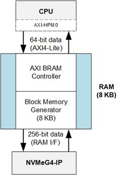
Figure 10 8KB RAM (True Dual Port)
The 8KB RAM is implemented using two AMD IP cores: the AXI BRAM Controller and the Block Memory Generator. This memory supports simultaneous write and read access by two masters: the CPU and the NVMeG4-IP.
· The AXI BRAM Controller IP acts as a bridge, converting the native RAM interface of the dual-port RAM into a 64-bit AXI4-Lite interface for communication with the CPU.
· The Block Memory Generator is configured as a true dual-port RAM with an 8 KB capacity and asymmetric data widths. One port uses a 256-bit interface, connected directly to the NVMeG4-IP, while the other uses a 64-bit interface for CPU access via the AXI BRAM Controller.
2.3 AXI DMA
The AMD LogiCORE™ AXI Direct Memory Access (AXI DMA) core is a soft IP core provided by AMD for use with the Vivado™ Design Suite. The AXI DMA provides high-bandwidth direct memory access between memory and AXI4-Stream target peripherals. It supports scatter/gather operations, helping to offload data movement tasks from the CPU. For more details about the AXI DMA IP core, refer to the AMD website:
https://www.amd.com/en/products/adaptive-socs-and-fpgas/intellectual-property/axi_dma.html
2.4 Processing system (PS)
The Processing System (PS) in a Zynq UltraScale+ MPSoC is a highly integrated and powerful multicore computing subsystem (CPU). It supports the execution of Linux through PetaLinux and provides robust system capabilities including general-purpose processing, real-time control, rich connectivity, and tight integration with programmable logic (PL). The PS also includes a high-performance memory (DDR) critical for operating system and data-intensive applications.
3 Software

Figure 11 Software Layer
To operate an NVMe SSD on a PetaLinux platform, the system software is structured into two primary layers: User Space and Kernel Space, as shown in Figure 11.
In the user space, the key components include the DG NVMe Application, which serves as an example application for working with the NVMeG4-IP on PetaLinux, and the DG NVMeG4 IP Library, which provides APIs for command generation and communication. This library enables the application to interact with the underlying kernel drivers and hardware, offering a simplified and structured interface for NVMe operations.
The Kernel Space contains two primary drivers: the DMA Dual Driver and the DG NVMeG4 Driver. The DMA Dual Driver manages high-speed data transfers through two AXI DMA channels, working in conjunction with the Linux DMA Engine Driver and the AMD DMA Driver to control hardware-level data movement between host memory and the NVMe SSD. The DG NVMeG4 Driver, on the other hand, is responsible for handling control commands. It serves as the interface between the DG NVMeG4 IP Library in user space and the AXINVMeG4IP in hardware.
3.1 Device Driver
To facilitate communication between the PetaLinux OS and the NVMeG4-IP hardware, two kernel-space character device drivers are implemented. Each driver plays a distinct role: the DMA Dual Driver manages high-speed data transfers via DMA, while the DG NVMeG4 Driver handles control operations and command execution for the NVMe interface. These drivers abstract the complexity of direct hardware interaction, enabling user-space applications to perform efficient storage operations through standard Linux system calls. The following subsections describe the design and functionality of each driver in detail.
3.1.1 DMA Dual Driver

Figure 12 DMA Dual Driver
The DMA dual driver is a kernel-space character device driver that acts as a bridge between user-space applications and the underlying hardware by leveraging the AMD DMA driver through the standard Linux DMA Engine API, which is provided by the DMA Engine driver. The DMA dual driver was inspired by https://xilinx-wiki.atlassian.net/wiki/spaces/A/pages/1027702787/Linux+DMA+From+User+Space+2.0, but has been specifically developed to interface with two AXI DMA IPs, namely “AXI DMA#0” and “AXI DMA#1”.
To optimize efficiency, the DMA Dual Driver implements a zero-copy DMA mechanism using memory-mapped buffers. Instead of copying data between kernel and user space, the driver allocates DMA buffers in kernel space are maps them directly into user space via the “mmap” system call. This approach significantly reduces CPU overhead and enhances throughput.
Each DMA engine allocates a dedicated buffer in kernel space, which is divided into two halves to enable double buffering. This technique allows one half of the buffer to be actively transferred while the other is simultaneously being filled or processed, ensuring a continuous and non-blocking data stream between the software and hardware.

Figure 13 DMA Dual Driver Memory Mapping
As illustrated in Figure 13, the mapped memory follows an interleaved striping pattern to further enhance performance. A stripe, defined as a small memory block (configured at 4 KB), is used to alternate data between the two DMA engines. When buffers are mapped to user space, the memory layout is arranged so that the first stripe comes from “DMA Buffer #0”, the second from “DMA Buffer #1”, the third from “DMA Buffer #0”, and so on. This interleaving spans the entire user buffer.
From the user-space perspective, this results in a logically continuous buffer that contains interleaved data from DMA buffer. This design enables parallel data access, balances memory traffic across both channels, and ensures that incoming data appears sequential to the application, even though it is sourced concurrently from two separate DMA engines.
The DMA dual driver is implemented using two source files:
1. Header File (axidma-dual.h)
This shared header file is used by both the kernel driver and user-space applications. It defines macros, data structures, and “ioctl” commands used by the DMA dual driver.
2. Source File (axidma-dual.c)
This file implements the kernel-space character device driver module that interfaces with the two AXI DMA IPs. It defines standard file operations that allow user-space applications to interact with the DMA device through system calls. The supported file operations include:
· “.open”: Invoked when the device is opened (e.g., open("/dev/dma_dual_tx0", O_RDWR)). This function sets up the device and links internal driver data to the file descriptor, enabling subsequent calls like “ioctl” and “mmap” to reference the correct DMA channel.
· “.release”: Called when the device is closed. It optionally handles resource cleanup if any resources were allocated during device operation.
· “.unlocked_ioctl”: The main control interface, used to handle special commands from user space to control how DMA transfer works. These commands are defined in “axidma-dual.h” and include:
· START_XFER: Starts a DMA transfer on one or both channels by configuring a scatter-gather (SG) list, generating DMA descriptors, and assigning a completion callback to monitor the transfer status—all depending on the size of the data being transferred.
· FINISH_XFER: Waits for any ongoing DMA transfers to finish.
· GET_BUFSIZE: Returns the size of the allocated DMA buffer for each AXI DMA, indicating how much memory is available for DMA operations.
·
“.mmap”: Maps the DMA buffer into user
space, enabling zero-copy access to the memory from the application. This
eliminates the need for intermediate data copies, achieving high-throughput
operation, as illustrated in Figure 13.
3.1.2 DG NVMeG4 Driver

Figure 14 DG NVMeG4 Driver
The DG NVMeG4 Driver provides a high-performance Linux kernel interface for controlling the NVMeG4-IP hardware core through a character device. It enables user-space applications to issue storage-level commands, such as Identify, Read, Write, Flush, Secure Erase, SMART, and Shutdown using standard Linux system calls like “ioctl” and “mmap”. This design enables efficient communication between the PetaLinux software and custom NVMe hardware implemented on the FPGA.
The DG NVMeG4 driver is implemented using two source files:
1. Header File (dg-nvmeg4drv.h)
A shared header file used by both the kernel driver and user-space applications. It defines macros, data structures, and “ioctl” command code specific to the DG NVMeG4 driver.
2. Source File (dg-nvmeg4drv.c)
This file implements the kernel-space character device driver module that interfaces directly with the AXINVMeG4IP hardware. It defines a set of standard file operations to allow user-space applications to interact with the NVMeG4-IP hardware via system calls. The supported file operations include:
· “.open”: Invoked when the device is opened (e.g., open("/dev/dgnvme0", O_RDWR It initializes the device context and links internal driver data to the opened file descriptor, enabling subsequent operations such as “ioct” to function correctly.
· “.release”: Called when the device is closed. It optionally handles resource cleanup if any resources were allocated during device operation.
· “.unlocked_ioctl”: The main control interface for handling NVMe commands from user space. Supported commands include:
· IDEN_CMD: Initiates an Identify command to retrieve controller or namespace information from the NVMe device.
· WR_CMD: Initiates a write operation to the NVMe device. The driver first receives the user-defined configuration via “ioctl”, and then executes the data transfer accordingly.
· RD_CMD: Initiates a read operation. Similar to WR_CMD, the driver parses the user-specified configuration before retrieving data from the device.
· SMART_CMD: Sends a SMART/Health command to obtain diagnostic and usage information about the NVMe device.
· FLUSH_CMD: Send a Flush command to ensure that all volatile cache data is safely written to non-volatile memory inside the NVMe device.
· SEC_ERS_CMD: Initiates a Secure Erase process to permanently remove all user data stored on the NVMe device.
· SHUTDOWN_CMD: Executes a Shutdown operation to safely power down the NVMe controller. After issuing this command, the device must be physically power-cycled (turned off and on again) before reuse.
· REGISTER_UAPP: Registers the current user-space process for asynchronous signal notifications (e.g., upon transfer completion or error). The process ID is provided via an “ioctl” call and stored within the driver.
· “.mmap”: Maps the NVMeG4-IP’s register space directly into the application's virtual address space. This enables user-space programs to read hardware status efficiently without repeated system calls.
3.2 Library
The NVMe access library is a user-space software module designed to interface with the custom NVMeG4-IP hardware controller provided by Design Gateway in a PetaLinux environment. It serves as an abstraction layer between user applications and the DG NVMeG4 kernel driver, simplifying the process of issuing commands, mapping hardware memory, and interpreting responses. This design allows users to avoid low-level memory manipulation and system calls by wrapping these operations in easy-to-use function calls. Internally, the library relies on standard Linux mechanisms such as “mmap” for memory mapping and “ioctl” for command execution.
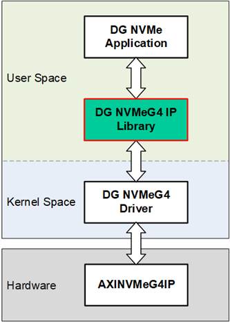
Figure 15 DG NVMeG4 Library
The library consists of the following files:
· Header File (dg-nvmeg4lib.h): Declares user-space data structures, function prototypes, and hardware-related constants required to communicate with the DG NVMeG4 driver and hardware registers.
· Source File (dg-nvmeg4lib.c): Implements the core logic of the user-space interface, including system call handling (e.g., open/close, ioctl command dispatch), memory mapping for 8KB RAM, and helper functions for parsing and displaying SMART and Identify data read from the hardware.
The functionality is categorized into three main groups:
1. Device Initialization/Cleanup Functions: These functions manage low-level setup and teardown of hardware access from user space. They handle opening character device file for both the NVMe controller and the mapped BRAM memory, and perform memory mapping using “mmap” to enable direct access to registers and data regions. Proper cleanup is also provided to unmap memory and close file descriptors.
2. NVMe Command Functions: These functions contain wrapper around NVMe command execution, such as Identify, Read, Write, SMART, Flush, Secure Erase, and Shutdown. Each function internally performs an “ioctl” call to the kernel driver, passing along required configuration structures. These functions allow users to issue NVMe commands using simple function calls.
3. Data Interpretation Functions: Once data is retrieved from the SSD via Identify or SMART command, it is stored in the 8KB RAM. This group of functions parses and formats the raw data into human-readable form. Additionally, it provides raw hexadecimal and ASCII display modes for debugging and analysis.
Device Initialization/Cleanup Functions
|
void open_dgnvme_devices(struct nvme_ip *nvme, char *nvme_name, struct bram *ram_8k, uint64_t bram_base_addr) |
|
|
Parameters |
nvme: Pointer to an “nvme_ip” structure containing general NVMe information. nvme_name: Character pointer to the path of the NVMe device file. ram_8k: Pointer to a “bram” structure managing the 8KB RAM. bram_base_addr: Physical base address for 8KB RAM mapping. |
|
Return value |
None |
|
Description |
Opens the device files for the NVMe device and 8 KB RAM, then maps them into user space using “mmap”. This enables direct access to NVMe registers and RAM from user applications without involving kernel-level copies. On failure to open or map, the function logs an error and exits using “exit(EXIT_FAILURE)”. |
|
int close_dgnvme_devices(struct nvme_ip *nvme, struct bram *ram_8k) |
|
|
Parameters |
nvme: Pointer to the “nvme_ip” structure containing general NVMe information. ram_8k: Pointer to the “bram” structure managing the 8 KB RAM. |
|
Return value |
0: Successful closure of devices and memory. -1: Error occurs during memory unmapping or file closing. |
|
Description |
Safely unmaps the previously mapped memory regions (both BRAM and register space) and closes the associated file descriptors. Each operation is guarded by error checking to ensure reliability. On error, an appropriate message is printed using “perror”, and “-1” is returned. |
|
void flush_cmd(struct nvme_ip *nvme) |
|
|
Parameters |
nvme: Pointer to the “nvme_ip” structure containing general NVMe information. |
|
Return value |
None |
|
Description |
Sends a flush command to the NVMe device using “ioctl”. This ensures that all cached data is committed to non-volatile storage. |
|
void iden_cmd(struct nvme_ip *nvme, struct bram *iden_ram) |
|
|
Parameters |
nvme: Pointer to the “nvme_ip” structure containing general NVMe information. iden_ram: Pointer to the “bram” structure used to access Identify data from the 8KB RAM. |
|
Return value |
None |
|
Description |
Sends an identify command to the NVMe device using “ioctl”. After that, it retrieves and stores model name, LBA configuration, and supported features. |
|
int read_cmd(struct nvme_ip *nvme, uint64_t addr, uint64_t length, uint32_t pktsize) |
|
|
Parameters |
nvme: Pointer to the “nvme_ip” structure containing general NVMe information. addr: Starting address of the data to be read (in 512-byte units). length: Length of the transfer (in 512-byte units). pktsize: DMA packet size (in 512-byte units). |
|
Return value |
0 on success An error code returned from “ioctl” if the input parameters are invalid. |
|
Description |
Configures and sends a Read command to the NVMe device. It sets the transfer parameters including address, length, and packet size. |
|
int sec_ers_cmd(struct nvme_ip *nvme) |
|
|
Parameters |
nvme: Pointer to the “nvme_ip” structure containing general NVMe information. |
|
Return value |
0: Secure Erase command was issued successfully. -1: Secure Erase is not supported by the device. |
|
Description |
Checks the “secure_erase_sup” flag in the “nvme” structure before issuing the Secure Erase command. If the feature is unsupported, an error message is printed and the function exits. Otherwise, the command is sent via “ioctrl”. |
|
void shutdown_cmd(struct nvme_ip *nvme) |
|
|
Parameters |
nvme: Pointer to the “nvme_ip” structure containing general NVMe information. |
|
Return value |
None |
|
Description |
Sends a Shutdown command to the NVMe device. It initiates a safe shutdown sequence. After execution, the device must be power-cycled before being used again. |
|
void smart_cmd(struct nvme_ip *nvme) |
|
|
Parameters |
nvme: Pointer to the “nvme_ip” structure containing general NVMe information. |
|
Return value |
None |
|
Description |
Sends a SMART command to the NVMe device. The response data, containing health and usage information, is read from the 8 KB RAM by interpretation functions such as “show_smart”. |
|
int write_cmd(struct nvme_ip *nvme, uint64_t addr, uint64_t length, uint32_t pktsize) |
|
|
Parameters |
nvme: Pointer to the “nvme_ip” structure containing general NVMe information. addr: Starting address of the data to be read (in 512-byte units). length: Length of the transfer (in 512-byte units). pktsize: DMA packet size (in 512-byte units). |
|
Return value |
0 on success An error code returned from “ioctl” if the input parameters are invalid. |
|
Description |
Configures and sends a Write command to the NVMe device. It sets the transfer parameters including address, length, and packet size. |
Data Interpretation Functions
|
void show_smart_size8byte(volatile unsigned char *char_ptr) |
|
|
Parameters |
char_ptr: Pointer to an 8-byte SMART log field |
|
Return value |
None |
|
Description |
Interprets the 8-byte value and converts this value to GB or TB. If the value exceeds the limit (500 PB), it prints overflow message. |
|
void show_smart_hex16byte(volatile unsigned char *char_ptr) |
|
|
Parameters |
char_ptr: Pointer of a 16-byte SMART log field |
|
Return value |
None |
|
Description |
Display the 16-byte value as hexadecimal unit. |
|
void show_smart_int8byte(volatile unsigned char *char_ptr) |
|
|
Parameters |
char_ptr: Pointer of 8-byte SMART log field |
|
Return value |
None |
|
Description |
If the input value is less than 4 billion (32-bit), the 8-byte SMART data is displayed in decimal units. Otherwise, an overflow message is displayed. |
|
void show_iden(struct nvme_ip *nvme, struct bram *iden_ram) |
|
|
Parameters |
nvme: Pointer to the “nvme_ip” structure containing general NVMe information. iden_ram: Pointer to the “bram” structure used to access Identify data from the 8 KB RAM. |
|
Return value |
None |
|
Description |
Displays SSD identification information from the provided ID data and NVMe IP structure. Prints the model number extracted from 8 KB RAM, calculates and shows capacity in gigabytes, displays LBA data size based on mode, and indicates support for the secure erase command. |
|
void show_id_smrt_raw(struct bram *ram_8k, uint32_t addr, uint32_t length) |
|
|
Parameters |
ram_8k: Pointer to the “bram” structure managing the 8KB RAM. addr: Start address (offset) in bytes from where data will be displayed. length: Number of bytes to display from the starting address. |
|
Return value |
None |
|
Description |
Displays a hex + ASCII dump of data from 8KB RAM, similar to hexdump tools. The function calculates the aligned starting row based on the address and prints 16 bytes per line. Each line shows offset, hexadecimal values, and ASCII equivalents. |
|
void show_smart(struct nvme_ip *nvme, struct bram *ctm_ram) |
|
|
Parameters |
nvme: Pointer to the “nvme_ip” structure containing general NVMe information. ctm_ram: Pointer to the “bram” structure used to access SMART log data from the 8 KB RAM. |
|
Return value |
None |
|
Description |
Parses and prints the SMART log in a user-friendly format. It extracts fields including Remaining life percentage, Device temperature, Total data read/written, and Power-on cycles. Additionally, it checks the critical warning byte and reports it if set. Internally, it reuses helper functions to format multi-byte values based on size and unit. |
3.3 Application
The DG NVMe Application is a user-space tool developed to interface with the NVMeG4-IP on a PetaLinux system. The application leverages supporting libraries introduced in the previous section to handle tasks such as memory mapping, register access, multi-threading, and formatted input/output. Upon execution, the application automatically checks for the presence and accessibility of the NVMe device before initiating any operation. It provides a command-line interface (CLI) with various subcommands, allowing users to interact with the SSD by issuing software-controlled instructions directly from user space.
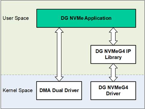
Figure 16 DG NVMe Application
3.3.1 NVMe Command
The DG NVMe Application is designed to support seven commands of the DG NVMeG4-IP: Identify, Read, Write, Flush, SMART, Secure Erase, and Shutdown. The usage and execution steps for each command are described as follows.
Identify Command
The Identify function retrieves NVMe Controller and Namespace data using the Identify command. It supports two output modes:
· Decoded Mode: Displays SSD information in a human-readable format, including Model Number, SSD Capacity, LBA Data Size, and Secure Erase support.
· Raw Mode: Outputs raw Identify data in hexadecimal format, based on a user-specified byte address and length.
The execution sequence for the identify command is as follows:
1) Receive the device path and user-defined options as input.
2) Initialize the NVMe and BRAM interfaces using “open_dgnvme_devices()”.
3) Issue the Identify command to the NVMe SSD using “iden_cmd()”.
4) Display the Identify data in the selected output mode (decoded or raw) parsed by “getopt_id()”.
5) Close the device interfaces and release resources using “close_dgnvme_devices()”.
The Write command is used to test data transfer performance by writing data to the NVMe SSD via DMA. It supports multiple data pattern modes, including perf, zero, one, inc, and dec. Users can configure the transfer offset and transfer length, both specified in units of 512 bytes. The execution sequence of the Write command is as follows:
1) Receive the device path and input options, including pattern mode, address, and length.
2) Initialize the NVMe and BRAM interfaces using “open_dgnvme_devices()”.
3) Allocate memory for the transmit buffer using “open_dma_devices()”.
4) Parse and validate the input parameters using “getopt_wr()”.
5) Issue the Write command to the NVMe SSD using “write_cmd()”.
6) Fill the transmit buffer with the selected data pattern and perform the transfer using “axi_wr()”, while displaying progress during execution.
7) Display the performance results upon completion.
8) Close device interfaces and free allocated memory using “close_dma_devices()” and “close_dgnvme_devices()”.
The Read command is used to test read performance or retrieve data from the NVMe SSD via DMA. It supports multiple operation modes, including perf, dump, zero, one, inc, and dec. Users can specify the transfer offset and transfer length in units of 512 bytes. The execution sequence of the Read command is as follows:
1) Receive the device path and input options, including pattern mode, address, and length.
2) Initialize the NVMe and BRAM interfaces using “open_dgnvme_devices()”.
3) Allocate memory for the receive buffer using “open_dma_devices()”.
4) Parse and validate the input parameters using “getopt_rd()”.
5) Issue the Read command to the NVMe SSD using “read_cmd()”.
6) Perform the data transfer and verify the received data using “axi_rd()”, while displaying progress during the operation.
7) Display the performance results upon completion.
8) Close device interfaces and free allocated memory using “close_dma_devices()” and “close_dgnvme_devices()”.
The SMART (Self-Monitoring, Analysis and Reporting Technology) command is used to retrieve health and usage information from the NVMe SSD. This information enables users to monitor the drive’s lifespan, usage history. It supports two output modes:
· Decoded Mode: Displays human-readable data extracted and decoded from the SMART log structure, typically used for monitoring device health and performance metrics.
· Raw Mode: Outputs raw SMART log data in hexadecimal format, based on a user-specified byte address and length.
The execution sequence of the SMART command is as follows:
1) Receive the device path and input options from the user.
2) Initialize the NVMe and BRAM interfaces using “open_dgnvme_devices()”.
3) Issue the SMART command to the NVMe SSD with “smart_cmd()”.
4) Display the SMART log based on the selected output mode (decoded or raw) parsed by “getopt_smrt()”.
5) Close the device interfaces and release resources using “close_dgnvme_devices()”.
The Secure Erase command is used to permanently remove all user data from the SSD. It is commonly performed to sanitize the drive before reusing it in another system. When supported, the NVMe controller may perform a cryptographic erase as part of this process. This command ensures that the data cannot be recovered through conventional means.
The execution sequence of the Secure Erase command is as follows:
1) Receive the device path and input options from the user.
2) Initialize the NVMe and BRAM interfaces using “open_dgnvme_devices()”.
3) Check for Secure Erase support and issue the command using “sec_ers_cmd()”.
4) Display progress messages until the operation completes.
5) Close the device interfaces and release resources using “close_dgnvme_devices()”.
The Flush command ensures that all data currently stored in the SSD’s volatile cache is written to non-volatile flash memory, guaranteeing data persistence. This operation is particularly important before powering down the system or shutting it down, as it helps to prevent potential data loss or corruption.
The execution sequence of the Flush command is as follows:
1) Receive the device path and input options from the user.
2) Initialize the NVMe and BRAM interfaces using “open_dgnvme_devices()”.
3) Issue the Flush command to the NVMe SSD using “flush_cmd()”.
4) Display progress messages until the operation completes.
5) Close the device interfaces and release resources using “close_dgnvme_devices()”.
The Shutdown command instructs the NVMe SSD to prepare for power down by safely flushing internal caches and performing any required shutdown routines. This process helps prevent data corruption and ensures the device transitions into a safe and stable power state.
The execution sequence of the Shutdown command is as follows:
1) Receive the device path and input options from the user.
2) Initialize the NVMe and BRAM interfaces using “open_dgnvme_devices()”.
3) Issue the Shutdown command to the NVMe SSD using “shutdown_cmd()”.
4) Display progress messages until the operation completes.
5) Close device interfaces and clean up using “close_dgnvme_devices()”.
3.3.2 Function List
This section describes the list of functions used to operate NVMeG4-IP.
|
int axi_wr(struct nvme_ip *nvme, struct dma_payload *d_pl) |
|
|
Parameters |
nvme: A pointer to a “nvme_ip” structure containing information about the NVMeG4-IP and mapped register addresses. d_pl: A pointer to a “dma_payload” structure that holds DMA configuration, buffer pointers, and data transfer parameters. |
|
Return value |
0: If the write operation completes successfully. -1: If device registration or thread creation fails. |
|
Description |
This function executes a write operation from main memory to the NVMe SSD using AXI DMA in a multi-threaded environment. It begins by registering the user-space application with the NVMe kernel driver to support interrupt-based status monitoring. Two threads are launched: one to handle the actual DMA write operation (write_dev), and another to track and display real-time progress information (transfer_progress). The function sets real-time scheduling priorities for these threads. Upon completion of both threads, the function checks the NVMe status register to verify the success of the operation. If the write is successful, it calculates and displays the overall transfer rate (in MB/s) along with the total elapsed time. |
|
int axi_rd(struct nvme_ip *nvme, struct dma_payload *d_pl) |
|
|
Parameters |
nvme: A pointer to a “nvme_ip” structure containing information about the NVMeG4-IP and mapped register addresses. d_pl: A pointer to a “dma_payload” structure that holds DMA configuration, buffer pointers, pattern mode, and transfer size. |
|
Return value |
0: If the read operation completes successfully. -1: If device registration or thread creation fails. |
|
Description |
This function performs a read operation from the NVMe SSD to main memory using AXI DMA in a multi-threaded setup. It begins by registering the user-space application with the NVMe kernel driver to support interrupt-based status monitoring. Depending on the selected read mode, the function adapts its execution path accordingly. If the mode is set to "dump", the function directly invokes dump_data() to read and display the data in hexadecimal format without launching DMA threads. For all other modes (e.g., perf, zero, one, inc, dec), the function creates two threads: one for managing the actual DMA read transfer (read_dev) and another for displaying real-time progress (transfer_progress). Real-time scheduling is applied to both threads. |
|
void* write_dev(void *arg) |
|
|
Parameters |
arg: A pointer to a user-defined structure that contains information required for the DMA transfer. |
|
Return value |
NULL |
|
Description |
This function is designed to execute in a separate thread and handle data transmission to a device using DMA. It reads the parameters from the provided structure and manages the setup and execution of the DMA write operation, including selecting the appropriate data pattern (e.g., perf, zero, inc), managing transfer alignment, and updating progress status. The function interacts directly with hardware or kernel-space driver interfaces to perform the write operation efficiently, often using memory-mapped buffers to minimize CPU overhead. |
|
void* read_dev(void *arg) |
|
|
Parameters |
arg: A pointer to a user-defined structure that contains information required for the DMA transfer. |
|
Return value |
NULL |
|
Description |
This function is designed to execute in a separate thread and handle data reception from a device using DMA. It reads the parameters from the provided structure and manages the setup and execution of the DMA read operation, including selecting the appropriate data pattern (e.g., perf, zero, inc), managing transfer alignment, and tracking read progress. The function interacts directly with hardware or kernel-space driver interfaces to perform the read operation efficiently, often using memory-mapped buffers to minimize CPU overhead. |
|
int decode_wr_mode(const char *target) |
|
|
Parameters |
target: A pointer to the string representing the write mode (e.g., “perf”, “zero”, “one”), which will be validated against the list of supported modes. |
|
Return value |
Index of Mode (0-4): If the input string matches a valid write mode. -1: If the input string does not match any supported mode. |
|
Description |
This function compares the input string against a predefined list of supported write modes: "perf", "zero", "one", "inc", and "dec". If a match is found, the corresponding index of that mode is returned, which is used internally by the application to configure the appropriate data pattern for DMA transfers. If the input string does not match any of the supported modes, the function returns -1 to indicate invalid input. |
|
int decode_rd_mode(const char *target) |
|
|
Parameters |
target: A pointer to the string representing the read mode (e.g., “perf”, “zero”, “one”, “dump”), which will be validated against the list of supported modes. |
|
Return value |
Index of Mode (0–5): If the
input string matches a valid read mode. |
|
Description |
This function compares the input string against a predefined list of supported read modes: "perf", "zero", "one", "inc", "dec", and "dump". If a match is found, the corresponding index of that mode is returned, which is used internally by the application to configure how data read from the NVMe device will be processed or displayed. The "dump" mode allows raw data to be output in hexadecimal format. If the input string does not match any of the supported modes, the function returns -1 to indicate invalid input. |
|
int getopt_id(int argc, char *argv[]) |
|
|
Parameters |
argc: The number of command-line arguments passed to the program. argv: An array of strings representing the command-line arguments. |
|
Return value |
0: If the command-line arguments were parsed successfully. 1: If an error occurred while parsing the arguments or invalid options were provided. |
|
Description |
This function parses the command-line arguments for the identify command. It interprets user input to determine whether the output should be displayed in decoded format (human-readable) or raw format (hexadecimal dump). The decoded format is triggered using the -d option, while the raw format requires the -r option followed by two arguments: the starting address and the length of data to display. If incorrect or missing arguments are provided, the function prints a usage message and returns a non-zero value to signal an error. |
|
int getopt_wr(int argc, char *argv[]) |
|
|
Parameters |
argc: The number of command-line arguments passed to the program. argv: An array of strings representing the command-line arguments. |
|
Return value |
0: If the command-line arguments were parsed successfully. 1: If an error occurred while parsing the arguments or if invalid input was detected. |
|
Description |
This function parses command-line arguments provided for the write command. It processes options for selecting the data pattern mode (-m), the starting block address (-a), and the total length of the transfer (-l). The pattern mode string is validated against a list of supported modes using decode_wr_mode(). The address and length arguments are validated to ensure correct formatting. If all options are parsed successfully, the function updates corresponding global variables with the selected configuration. If an invalid option or value is encountered, an error message is displayed and the function returns a non-zero value to indicate failure. |
|
int getopt_rd(int argc, char *argv[]) |
|
|
Parameters |
argc: The number of command-line arguments passed to the program. argv: An array of strings representing the command-line arguments. |
|
Return value |
0: If the command-line arguments were parsed successfully. 1: If an error occurred while parsing the arguments or if invalid input was detected. |
|
Description |
This function parses the command-line arguments for the read command. It interprets input parameters such as the read mode (-m), starting block address (-a), and length of data to read (-l). The read mode string is validated using decode_rd_mode() to ensure it matches one of the supported modes, including "dump" for hex data display. If "dump" mode is selected, the function bypasses the length validation since the length parameter is not required. For other modes, both the address and length are validated. If the arguments are parsed correctly, the function updates global variables with the appropriate values. If any input is missing or malformed, it prints a usage message and returns a non-zero value to indicate an error. |
|
int getopt_smrt(int argc, char *argv[]) |
|
|
Parameters |
argc: The number of command-line arguments passed to the program. argv: An array of strings representing the command-line arguments. |
|
Return value |
0: If the command-line arguments were parsed successfully. 1: If an error occurred while parsing the arguments or if invalid input was detected. |
|
Description |
This function parses command-line arguments provided for the smart command. It supports two output modes: decoded mode, activated with the -d option, which presents SMART log data in a human-readable format; and raw mode, triggered with the -r option, which requires an additional starting address and length in bytes to display the raw SMART log data in hexadecimal. The function validates the input values and prints a usage message if any required parameter is missing or malformed. A return value of zero indicates successful parsing, while a non-zero value signals an error. |
Device Installation and Clean Up Function
|
int close_dma_devices(struct dma_payload *d_pl) |
|
|
Parameters |
d_pl: A pointer to a “dma_payload” structure that holds DMA configuration and buffer pointers. |
|
Return value |
0: If the DMA devices and associated memory regions were successfully closed and unmapped. -1: If an error occurred while closing the DMA devices. |
|
Description |
This function performs cleanup of the DMA environment by properly releasing all allocated resources. It begins by unmapping the transmit and receive buffers from user space using munmap(), based on the buffer pointers and sizes stored in the dma_payload structure. After unmapping, it closes the corresponding file descriptors for the transmit (fd_tx) and receive (fd_rx) DMA channels. A return value of 0 indicates successful cleanup, while -1 signifies that one or more resources could not be released properly. |
|
void open_dma_devices(struct dma_payload *d_pl) |
|
|
Parameters |
d_pl: A pointer to a “dma_payload” structure that holds DMA configuration and buffer pointers. |
|
Return value |
None |
|
Description |
This function initializes the DMA environment required for high-speed data transfers. It opens both the transmit (/dev/dma_dual_tx0) and receive (/dev/dma_dual_rx0) character device files, which are associated with the dual AXI DMA driver. After successfully opening the device files, it performs memory mapping using the mmap() system call to map the DMA buffers into the user space. The function updates the dma_payload structure with relevant buffer pointers and buffer size information. If any step fails—such as device file access or memory mapping—the function prints an error message and terminates the program to prevent further execution with an invalid DMA configuration. |
Pattern Generator and Checker Function
|
void chk_dec(uint32_t *arr, int count, uint32_t *offset) |
|
|
Parameters |
arr: A pointer to the array containing the 32-bit values to be verified. count: The number of elements in the array to check against the expected decremental pattern. offset: A pointer to a 32-bit value representing the starting point of the expected pattern. |
|
Return value |
None |
|
Description |
This function verifies data by comparing each 32-bit element in the input array against an expected decremental sequence. The expected values begin from the value pointed to by offset, which is decremented after each comparison. If any mismatch is detected between the actual and expected values, the function logs a detailed error message including the mismatched values. This function is typically used in verification scenarios where data was written using a decremental pattern. |
|
void chk_inc(uint32_t *arr, int count, uint32_t *offset) |
|
|
Parameters |
arr: A pointer to the array containing the 32-bit values to be verified. count: The number of elements in the array to check against the expected incremental pattern. offset: A pointer to a 32-bit value representing the starting point of the expected pattern. |
|
Return value |
None |
|
Description |
This function verifies data by comparing each 32-bit element in the input array against an expected incremental sequence. The expected values begin from the value pointed to by offset, which is incremented after each comparison. If any mismatch is detected between the actual and expected values, the function logs a detailed error message including the index and the mismatched values. This function is typically used in verification scenarios where data was written using an incremental pattern. |
|
void chk_one(uint32_t *arr, int count) |
|
|
Parameters |
arr: A pointer to the array containing the 32-bit values to be verified. count: The number of elements in the array to check. |
|
Return value |
None |
|
Description |
This function validates that every 32-bit value in the given array is equal to the all-one pattern (FFFF_FFFFh). It iterates through the array and compares each element against this fixed value. If a mismatch is found, the function prints a detailed error message including the incorrect value and the expected value. |
|
void chk_zero(uint32_t *arr, int count) |
|
|
Parameters |
arr: A pointer to the array containing the 32-bit values to be verified. count: The number of elements in the array to check. |
|
Return value |
None |
|
Description |
This function verifies that each element in the input array contains the fixed all-zero value (0000_0000h). It iterates through all count elements of the array and compares each value against zero. If any mismatch is detected, an error message is printed specifying the actual value found and the expected value. |
|
void gen_inc(uint32_t *arr, int count, uint32_t *offset) |
|
|
Parameters |
arr: A pointer to the array where the generated incremental pattern will be stored. count: The number of 32-bit values to generate and store in the array. offset: A pointer to a 32-bit value used to change the generated numbers. |
|
Return value |
None |
|
Description |
This function fills the specified array with a sequence of incrementing 32-bit unsigned integers. The sequence starts from the value pointed to by offset and continues for count elements. After generating the pattern, the offset is updated to reflect the next value in the sequence. This pattern is commonly used in write operations. |
|
void gen_dec(uint32_t *arr, int count, uint32_t *offset) |
|
|
Parameters |
arr: A pointer to the array where the generated decremental pattern will be stored. count: The number of 32-bit values to generate and store in the array. offset: A pointer to a 32-bit value used to change the generated numbers. |
|
Return value |
None |
|
Description |
This function generates a sequence of 32-bit unsigned integers in descending order and stores them into the given array. The sequence begins from the value pointed to by “offset” and decrements with each element generated, continuing for the specified “count”. After the pattern is created, the offset is updated to the next starting value in the sequence. |
|
void print_fail(uint32_t data, uint32_t offset) |
|
|
Parameters |
data: The 32-bit actual value obtained from the array or de vice during verification. offset: The 32-bit expected value that the actual value is compared against. |
|
Return value |
None |
|
Description |
This utility function prints an error message when a mismatch is detected during pattern verification. It displays both the actual value (data) and the expected value (offset) in hexadecimal format. The function is typically called from within validation routines like chk_inc(), chk_dec(), chk_zero(), or chk_one() whenever data integrity checks fail. |
Progress Monitoring and Timing Function
|
void* ctm_cmd_progress(void) |
|
|
Parameters |
None |
|
Return value |
NULL |
|
Description |
This function is designed to monitor and display the runtime duration of NVMe commands, such as Flush, SMART, Secure Erase, and Shutdown. It operates in a separate thread and repeatedly prints the number of seconds elapsed since the command started. The runtime counter is updated every second until the operation completes. |
|
uint64_t get_posix_clock_time_usec(void) |
|
|
Parameters |
None |
|
Return value |
Current time: Measured in microseconds, as a 64-bit unsigned integer. 0: If an error occurs while accessing the clock. |
|
Description |
This utility function retrieves the current time using the POSIX clock_gettime() function. The function converts the result to microseconds for use in performance measurement or progress reporting. If the system fails to retrieve the time, the function returns 0 as an error indicator. |
|
void* transfer_progress(void *arg) |
|
|
Parameters |
arg: A pointer to the “nvme_ip” structure containing state for the NVMeG4-IP. |
|
Return value |
NULL |
|
Description |
This function runs in a separate thread to continuously monitor and display the progress of a data transfer operation in real time. It retrieves the remaining transfer length from NVMeG4-IP hardware registers, calculates the percentage of data transferred, and reports the elapsed time and estimated transfer speed. Updates are printed to the console once per second. The function terminates once the transfer is complete or an error is detected, offering a non-blocking way to track DMA write or read operations in parallel with their execution. |
Utility and System Control Function
|
int ctm_cmd_pending(struct nvme_ip *nvme) |
|
|
Parameters |
nvme: A pointer to a “nvme_ip” structure containing information about the NVMeG4-IP and mapped register addresses. |
|
Return value |
0: If the pending command handler is successfully set up. -1: If any error occurs during the thread creation or initialization. |
|
Description |
This utility function is used to track the progress of
NVMe commands—such as Flush, Secure Erase, SMART, or Shutdown—by launching a
separate thread to display runtime status. It starts by registering the
current application with the NVMe device (via ioctl) to allow asynchronous
status updates or signal handling. |
|
char get_keypress(void) |
|
|
Parameters |
None |
|
Return value |
The character input by the user as a “char”. The input is captured immediately without waiting for the Enter key. |
|
Description |
This utility function captures a single keystroke from
the terminal in non-canonical mode (also known as raw or unbuffered input
mode). It temporarily modifies the terminal attributes to disable both line
buffering (canonical mode) and input echo, allowing the program to receive
immediate input from the user. |
|
void hex_dump(const void *data, uint64_t addr, uint64_t length) |
|
|
Parameters |
data: A pointer to the memory buffer to be dumped, pointing to data to be displayed. addr: The starting memory address of the data to be displayed. length: The number of bytes to display starting from the “data” pointer. |
|
Return value |
None |
|
Description |
This utility function produces a structured and readable hexadecimal dump of a specified memory region. It prints the address, the hexadecimal values, and ASCII representation. This format makes it easier to inspect binary memory regions for debugging, logging, or verifying hardware data exchanges. |
|
void progress_end(int sig) |
|
|
Parameters |
sig: An integer representing the signal number received. |
|
Return value |
None |
|
Description |
This function acts as a signal handler that is triggered when a monitored data transfer or NVMe command execution completes. Upon receiving a signal, it performs the following actions: · Reads the final user status from the NVMe IP’s control registers to determine whether the operation completed successfully or with an error. · Computes the total runtime of the operation using the internal timer initialized when the operation began. · Based on the operation type (e.g., write, read, flush) and verification mode, it decides whether to display final progress and performance statistics. · Conditionally shows a summary of success or failure. |
|
void sigint(int a) |
|
|
Parameters |
a: An integer representing the signal number received. Typically, this corresponds to SIGINT (usually triggered by pressing Ctrl+C). |
|
Return value |
None |
|
Description |
This function serves as a signal handler for the interrupt signal SIGINT. When the user manually interrupts the program (e.g., by pressing Ctrl+C), the function is invoked to initiate a controlled shutdown or halt of ongoing operations. It sets the global variable stop to 1, which can be checked by other parts of the application (such as data transfer loops or command threads) to safely exit their execution. This design allows for termination of processes. |
Command-Line Help and Usage Display Functions
|
void print_help(void) |
|
|
Parameters |
None |
|
Return value |
None |
|
Description |
This function prints the general usage information for the dgnvme command-line tool. It provides a summary of all supported commands such as identify, read, write, flush, smart, secure-erase, and shutdown. Each command is listed with a brief explanation of its functionality, helping users understand the tool’s capabilities. The function also directs users on how to obtain detailed help for specific commands, typically by invoking dgnvme help <command>. |
|
void print_help_flush(void) |
|
|
Parameters |
None |
|
Return value |
None |
|
Description |
This function prints the usage guide for the flush command to the terminal. It provides the correct syntax for invoking the command. It is typically called when the user provides incorrect arguments or explicitly requests help for the flush command. |
|
void print_help_identify(void) |
|
|
Parameters |
None |
|
Return value |
None |
|
Description |
This function displays the usage instructions for the identify command of the dgnvme application. It explains how users can retrieve NVMe device information in either a human-readable (decoded) or raw hexadecimal format. The help text outlines the required syntax for both output modes and provides example command lines to guide proper usage. |
|
void print_help_write(uint64_t capacity, bool dev_def) |
|
|
Parameters |
capacity: The total capacity of the NVMe device in bytes. dev_def: A flag indicating whether to print the capacity at the end of the help message. |
|
Return value |
None |
|
Description |
This function prints detailed usage instructions for the write command in the dgnvme application. It explains how to initiate a write operation using different pattern modes (perf, zero, one, inc, dec) and guides users on specifying the target device, start address, and data length—both expressed in 512-byte units. If the dev_def flag is set to true, the help message concludes by showing the total capacity of the device, helping users avoid exceeding its limits. |
|
void print_help_read(uint64_t capacity, bool dev_def) |
|
|
Parameters |
capacity: The total capacity of the NVMe device in bytes. dev_def: A flag indicating whether to print the capacity at the end of the help message. |
|
Return value |
None |
|
Description |
This function displays usage instructions for the read command in the dgnvme application. It outlines the valid read pattern modes (perf, zero, one, inc, dec) along with a dump mode that outputs raw data in hexadecimal format to the console. It also explains how to specify the start address and data length for the operation—both in 512-byte units. If the dev_def flag is set to true, the help message concludes by showing the total capacity of the device, helping users avoid exceeding its limits. |
|
void print_help_secure_erase(void) |
|
|
Parameters |
None |
|
Return value |
None |
|
Description |
This function displays the usage instructions for the secure-erase command in the dgnvme application. It explains the syntax required to issue a secure erase operation. The help message includes an example command to illustrate correct usage. |
|
void print_help_shutdown(void) |
|
|
Parameters |
None |
|
Return value |
None |
|
Description |
This function displays the usage instructions for the shutdown command within the dgnvme application. It explains how to properly initiate a safe shutdown procedure for the NVMe SSD. The help text includes the correct syntax for issuing the command and provides a usage example to guide the user. |
|
void print_help_smart(void) |
|
|
Parameters |
None |
|
Return value |
None |
|
Description |
This function prints the usage instructions for the smart command in the dgnvme application. It guides users on how to retrieve SSD health information using SMART. The help message explains the two output modes—decoded and raw—and provides details on how to specify byte offsets and lengths for the raw mode. |
4 Example Test Result
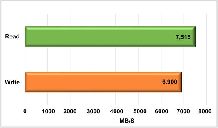
Figure 17 Test Performance on PetaLinux with NVMeG4-IP Using Samsung 990 Pro SSD
Figure 17 presents the performance results of Write and Read operations executed on the demo system, which utilizes a 1 TB Samsung 990 Pro SSD and the NVMeG4-IP configured with a 1 MB buffer, running on a PetaLinux platform. The evaluation was performed in performance mode, where the CPU is excluded from data generation and verification processes in order to demonstrate the maximum achievable performance. The write performance reaches approximately 6900 MB/s, while the read performance achieves around 7500 MB/s.
5 Revision History
|
Revision |
Date (D-M-Y) |
Description |
|
1.00 |
26-Jun-25 |
Initial version release |