muNVMe-IP for Gen4 reference design manual
Rev1.0 8-Aug-23
2.2.2 Integrated Block for PCIe
3.1 Test firmware (munvmeiptest.c)
3.2 Function list in Test firmware
1 Overview
The NVMe-IP for Gen4 currently utilizes a single user interface, allowing the transmission of one command at a time. Consequently, users are unable to simultaneously issue Write and Read commands to access distinct areas of the same SSD. In order to address this limitation, the muNVMe-IP for Gen4 (multiple-user NVMe-IP for Gen4 speed) has been developed, featuring four user interfaces that enable the concurrent transmission of up to four Write/Read commands to the same SSD.
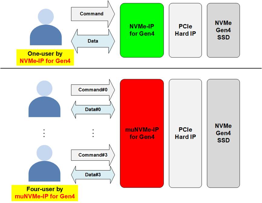
Figure 1‑1 NVMe-IP for Gen4 and muNVMe-IP for Gen4 comparison
The users allow to adjust the number of user interfaces to be 2, 3, or 4 by assigning the corresponding parameters in the HDL code. Similarly, the buffer size within muNVMe-IP for Gen4 can be configured by modifying the parameters in the HDL code. Opting for smaller buffer sizes and a reduced number of user interfaces leads to lower FPGA resource utilization.
Each user interface within muNVMe-IP for Gen4 operate independently, allowing users to request command values individually. Consequently, users have the flexibility to send the same command or different commands across all user interfaces. This means that they can send commands such as four Write commands, four Read commands, or a combination of two Write and two Read commands. In scenarios where all interfaces execute the same command, the write or read performance of each user interface is approximately one-fourth of the maximum performance achievable with a single user interface. However, when executing mixed Write-Read command commands, the performance is contingent upon the characteristics of the SSD being used.
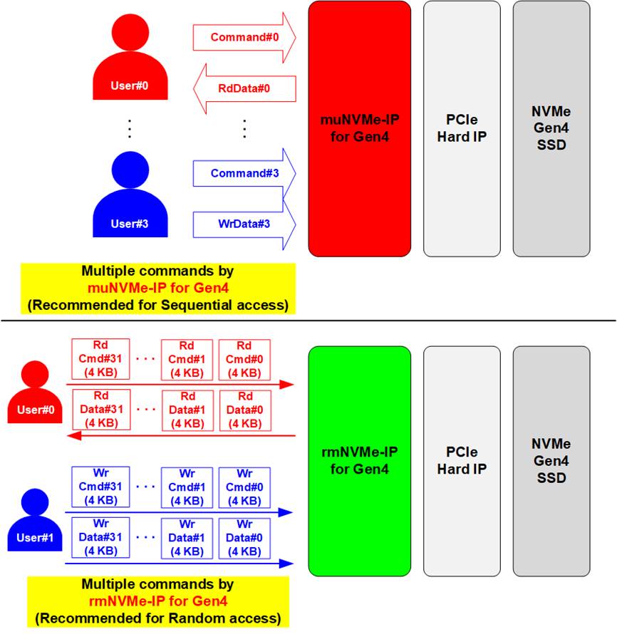
Figure 1‑2 muNVMe-IP for Gen4 and rmNVMe-IP for Gen4 comparison
Design Gateway offers an additional IP solution known as rmNVMe-IP, which features two user interfaces. User#0 interface is dedicated to Read commands, while User#1 interface handles Write commands. rmNVMe-IP is specifically designed to facilitate random access by setting a fixed data size of 4 Kbytes for each command. This IP solution supports simultaneous Write and Read commands, making it well-suited for applications that requires random access functionality. In contrast, muNVMe-IP matches the applications that prioritize sequential Write and Read commands, as it enables higher performance compared to random access scenarios.
2 Hardware overview
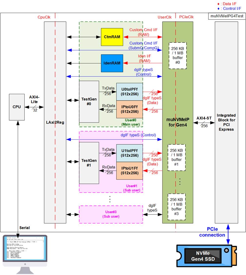
Figure 2‑1 muNVMe-IP for Gen4 demo hardware
This reference design showcases the configuration of muNVMe-IP for Gen4 with four user interfaces using two buffer modes, 256 KB and 1 MB per user. In most cases, SSDs exhibit enhanced Write/Read performance when a 1 MB buffer is utilized.
Figure 2‑1 presents a block diagram illustrating the submodule details within the reference design. The submodule can be categorized into different functional groups. The test function comprises TestGen, which connects to the user interface of muNVMe-IP. The NVMe function encompasses CtmRAM, IdenRAM, U0-U3toIPFf, IPtoU0-U3Ff, muNVMe-IP for Gen4, and PCIe Hard IP, responsible for handling NVMe and PCIe protocols. Lastly, the CPU system comprises the CPU and LAxi2Reg, which receive test parameters from the user and display test results. In real systems, the CPU system can be omitted, integrating simple logic instead to assign test parameters.
TestGen functions as the test logic, generating a test data stream for muNVMe-IP via U0-U3toIPFf during Write command execution and reading the data stream output from muNVMe-IP via IPtoU0-U3Ff for verification during Read command execution. Each TestGen module connects with one user interface of muNVMe-IP for Gen4, resulting in the integration of four TestGen modules that run independently. User can assign the maximum data rate transferred in Write/Read commands for each TestGen in the test environment.
NVMe encompasses muNVMe-IP and the PCIe hard IP (Integrated Block for PCI Express), enabling direct access to NVMe Gen4 SSD without PCIe switch. CtmRAM and IdenRAM are included to store health data from the SMART command and SSD information from the Identify command, respectively. Two FIFOs are employed for each user interface (UtoIPFf and IPtoUFf) as examples of the data interface in muNVMe-IP for simple control logic.
The CPU is connected to LAxi2Reg module for interface with the NVMe test logics. Integrating CPU to the test system allows the user to set the test parameters and monitor the test status via Serial console. Using CPU also facilitates the execution of multiple test cases to verify the functionality of the IP. The default firmware for the CPU includes the functions for executing the NVMe commands using muNVMe-IP
There are three clock domains shown in Figure 2‑1: CpuClk, UserClk, and PCIeClk. CpuClk is the clock domain for the CPU and its peripherals, and it must be a stable clock that can be independent from other hardware. The UserClk is the user clock domain utilized for the operation of the muNVMe-IP, RAM, FIFO, and TestGen. As specified in muNVMe-IP datasheet, the clock frequency of UserClk must be greater than or equal to PCIeClk frequency. The reference design utilizes 275 MHz for UserClk. Finally, the PCIeClk is the clock output generated by the PCIe hard IP, which is synchronized with the 256-bit AXI4 stream. The frequency of PCIeClk is 250 MHz for for 4-lane PCIe Gen4.
Further hardware details are described in the following sections.
2.1 TestGen
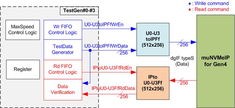
Figure 2‑2 TestGen interface
The TestGen module handles the data interface of muNVMe-IP, facilitating data transfer for both Write and Read commands. In case of a Write command, TestGen sends 256-bit test data to muNVMe-IP via U0-U3toIPFf. In contrast, for a Read command, the test data is received from IPtoU0-U3Ff for comparison with the expected value, ensuring data accuracy.
Within this block, there is a MaxSpeed Control Logic that generates an enable pulse to regulate the number of clock cycles in which 1b is asserted out of every 100 clock cycles. This enable pulse is then fed to both Wr and Rd FIFO Control Logics, enabling control over the maximum data rate ruing Write/Read data transfers. The Wr and Rd FIFO Control Logics assert the write enable and the read enable signals when the FIFO is ready, and the enable pulse from the MaxSpeed Control Logic is activated.
The Register file in the TestGen receives various test parameters from the user, including the total transfer size, transfer direction, verification enable, test pattern selector, and transfer rate. For further details of the hardware logic of TestGen, refer to Figure 2‑3.
Figure 2‑3 TestGen hardware
The MaxSpeed Control Logic is implemented using a counter called MaxSpeed Counter and a decoder to assert rTrnRateEn to 1b. The value of TrnRate input determines the number of cycles in which rTrnRateEn is asserted to 1b out of every 100 clock cycles. The counter operates when either a Write or Read command is in progress (rWrTrans=1b or rRdTrans=1b). By monitoring rTrnRateCnt, rTrnRateEn can be asserted to 1b or de-asserted to 0b at specific times to control the maximum data rate. The enable signals for the Write and Read FIFO are only asserted when rTrnRateEn is set to 1b.
The primary flow control signal for the Write command is WrFfAFull, while for the Read command, it is RdFfEmpty. In the case of a Write command, WrFfAFull is de-asserted to 0b when there is free space in the Write FIFO beyond a certain threshold. When WrFfAFull=0b and rTrnRateEn=1b, WrFfWrEn is asserted to 1b to send Write data to the FIFO. For a Read command, RdFfEmpty is de-asserted to 0b when there is available data in the Read FIFO. When RdFfEmpty=0b and rTrnRateEn=1b, RdFfRdEn is asserted to 1b to read data from the FIFO.
The user can configure four test parameters: total transfer size (TrnLen), start address (TrnAddr), test pattern selector (PattSel), and transfer rate (TrnRate). TrnLen is fed to the calculating unit to determine the end position (rEndSize) for comparison with the Data counter.
The “TestData Generator” subblock is responsible for generating the test data (WrData) that will be transmitted to muNVMe-IP during the Write command. Each 512-byte data segment comprises a 64-bit header data and a test pattern, selected by the PattSel parameter.
Figure 2‑4 Test pattern format in each 512-byte data for Increment/Decrement/LFSR pattern
As shown in Figure 2‑4, the 64-bit header at DW#0 (Dword#0) and DW#1 is generated by combining the 48-bit address, retrieved from the HdrFIFO, with a zero value. The remaining data (DW#2 – DW#1023) represents the test pattern, which can be chosen from three different formats: 32-bit incremental data, 32-bit decremental data, and 32-bit LFSR counter. The 32-bit incremental data is derived from the output of the Data Counter. The decremental data is obtained by applying the logical NOT operation to the incremental data. The LFSR data is generated using the Fibonacci LFSR algorithm, following the equation x^31 + x^21 + x + 1.
To implement the 256-bit LFSR pattern, the data is divided into two sets of 128-bit data, each having a distinct initial value. The 128-bit data employs a look-ahead technique to calculate four 32-bit LFSR data in one clock cycle. As illustrated in Figure 2‑5, the initial value of the LFSR is determined by combining a portion of the lower 32 bits of the LBA address (LBAAddr) with the logical NOT of the lower 32 bits of the LBA address (LBAAddrB).
In case of the all-zero and all-one patterns, a 64-bit header is not included within the 512-byte data. These patterns are often used to assess the optimal Write/Read performance of certain SSDs.
Figure 2‑5 256-bit LFSR Pattern in TestGen
The generated test data serves as the Write data for the FIFO (rWrFfWrData) during the Write command, or it is used as the expected data for verification against the read data obtained from the FIFO (RdFfRdData) during the Read command. In the event of a verification failure, the failure flag (PattFail) is asserted to 1b. The timing diagram for writing data to the FIFO during the Write command is shown in Figure 2‑6.
Figure 2‑6 Timing diagram of Write command in TestGen
1) The operation begins when WrPattStart is asserted to 1b. This signal remains asserted for only one clock cycle. Subsequently, rWrTrans is set to 1b, indicating that Write request is in progress. It is de-asserted upon completion of the operation.
2) While rWrTrans is set to 1b, rTrnRateCnt counts up from 1 to 100. The initial value of rTrnRateCnt is 100. When rWrTrans=1b and rTrnRateCnt=100, rTrnRateEn is asserted to 1b.
3) When both rWrTrans and rTrnRateEn are asserted to 1b, and the FIFO is not full (WrFfAFull=0b), rWrFfWrEn is asserted to 1b, allowing the test data to be written to FIFO.
4) The data counter (rDataCnt) increments when rWrFfWrEn is asserted to 1b. Therefore, it can be monitored to determine the total amount of data transmitted to the FIFO.
5) In this example, TrnRate is set to 40, resulting in a maximum data rate of approximately 40/100 = 40% of the logic’s maximum throughput. rTrnRateEn is asserted to 1b for 40 cycles out of every 100 cycles. Once rTrnRateCnt=40, rTrnRateEn is de-asserted to 0b.
6) When rTrnRateEn is de-asserted to 0b, rWrFfWrEn is also de-asserted to 0b, temporarily pausing the transmission of data.
7) If the FIFO becomes full (WrFfAFull=1b), the writing process is paused by de-asserting rWrFfWrEn to 0b. rWrFfWrEn is re-asserted to 1b when WrFfAFull is de-asserted to 0b.
8) Once the total data count (rDataCnt) equals to the total transfer size (rEndSize), both rWrTrans and rWrFfWrEn are de-asserted to 0b, indicating the completion of the Write command.
Figure 2‑7 Timing diagram of Read command in TestGen
1) The operation begins when RdPattStart is asserted to 1b. This signal remains asserted for only one clock cycle. Subsequently, rRdTrans is asserted to 1b to control rTrnRateEn It is de-asserted once all data has been completely transferred.
2) While rRdTrans is set to 1b, rTrnRateCnt increments from 1 to 100. The initial value of rTrnRateCnt is 100. If rRdTrans=1b and rTrnRateCnt=100, rTrnRateEn is asserted to 1b.
3) When rTrnRateEn is asserted to 1b and the FIFO contains data (RdFfEmpty=0b), RdFfRdEn is asserted to 1b, enabling the reading of test data from the FIFO.
4) The data counter (rDataCnt) increments after RdFfRdEn is asserted to 1b for two clock cycles. It can be monitored to determine the total amount of received data from the FIFO.
5) In this example, TrnRate is set to 40, resulting in a maximum data rate of approximately 40/100 = 40% of the logic’s maximum throughput. rTrnRateEn is asserted to 1b for 40 cycles out of every 100 cycles. Once rTrnRateCnt=40, rTrnRateEn is de-asserted to 0b.
6) If rTrnRateEn is de-asserted to 0b, RdFfRdEn is also de-asserted to 0b, pausing the transmission of data in the same clock cycle.
7) If the FIFO is empty (RdFfEmpty=1b), the reading process is paused by de-asserting RdFfRdEn to 0b. RdFfRdEn is re-asserted to 1b when RdFfEmpty is de-asserted to 0b.
8) Once the total data count (rDataCnt) equals the total transfer size (rEndSize), rRdTrans is de-asserted to 0b, indicating the completion of the Read command.
2.2 NVMe
Figure 2‑8 NVMe hardware
Figure 2‑8 illustrates the integration of muNVMe-IP for Gen4 into the reference design. Each user interface of muNVMe-IP consists of a Control interface and a Data interface. The Control interface of User#0 supports to reception of commands and parameters through either the Custom command interface or dgIF typeS. The Custom command interface is utilized when operating SMART or Flush command. On the other hand, the Control interfaces of User#1 - #3 only have dgIF typeS to support Write and Read commands.
The Data interface of User#0 comprises four interfaces: the Custom command RAM interface, Identify interface, FIFO input interface (dgIF typeS), and FIFO output interface (dgIF typeS). The data interfaces of User#1 - #3 include FIFO input and output interfaces (dgIF typeS). All data interfaces have a data bus width of 256 bits. The Custom command RAM interface is a bi-directional interface, while the other interfaces are unidirectional interface. In the reference design, the Custom command RAM interface is employed for data transfer in the receive direction (storing SMART data transferred from muNVMe-IP to LAxi2Reg).
2.2.1 muNVMe-IP for Gen4
The muNVMe-IP implements the NVMe protocol on the host side, enabling direct access to an NVMe SSD without a PCIe switch. The muNVMe-IP for Gen4 provides four user interfaces, allowing for the concurrent execution of up to four commands. The first user, known as the Main user, supports six commands: Write, Read, Identify, Shutdown, SMART, and Flush. The 2nd to 4th users, referred to as Sub users, support two commands: Write and Read. The PCIe interface of the muNVMe-IP can be directly connected to the PCIe hard IP. For more detailed information about the muNVMe-IP, please refer to the datasheet available at the following link.
https://dgway.com/products/IP/NVMe-IP/dg_munvme_ip_data_sheet_g4_xilinx.pdf
2.2.2 Integrated Block for PCIe
This block refers to the hard IP integrated into certain Xilinx FPGAs to support PCIe Gen4 speed. It encompasses the Physical, Data Link, and Transaction Layers of the PCIe specification. More detailed information can be found in the Xilinx documents.
PG213: UltraScale+ Devices Integrated Block for PCI Express
https://www.xilinx.com/products/intellectual-property/pcie4-ultrascale-plus.html#documentation
PG343: Versal ACAP Integrated Block for PCI Express
https://www.xilinx.com/products/intellectual-property/pcie-versal.html#documentation
The PCIe hard IP is generated using the IP wizard. It is recommended for user to select a “PCIe Block Location” that is in close proximity to the transceiver pin connecting to the SSD. Further details regarding the location of PCIe hard IP and the transceiver can be found in the following document.
UG575: UltraScale and UltraScale+ FPGAs Packaging and Pinouts
https://www.xilinx.com/support/documentation/user_guides/ug575-ultrascale-pkg-pinout.pdf
AM013: Versal ACAP Packaging and Pinouts
https://www.xilinx.com/support/documentation/architecture-manuals/am013-versal-pkg-pinout.pdf
An example of the PCIe hard IP location on the XCVC1902-VSVA2197 is shown in Figure 2‑9.
Figure 2‑9 PCIe Hard IP Pin location
2.2.3 Dual port RAM
Two dual port RAMs, CtmRAM and IdenRAM, store the returned data from Identify command and SMART command, respectively. IdenRAM has an 8 Kbyte size and is used to store the 8 Kbyte output from the Identify command. The data bus size for muNVMe-IP and LAxi2Reg differ, with muNVMe-IP having a 256-bit size and LAxi2Reg having a 32-bit size. As a result, IdenRAM is an asymmetric RAM with different bus sizes for its Write and Read interfaces. muNVMe-IP also has a double-word enable, which allows it to write only 32-bit data in certain cases. The RAM setting on Xilinx IP tool supports write byte enable, so a small logic circuit was designed to convert the double word enable to be write byte enable, as shown in Figure 2‑10.
Figure 2‑10 Byte write enable conversion logic
The input to the AND logic is bit[0] of WrDWEn and the WrEn signal. The output of the AND logic is fed to bit[3:0] of IdenRAM byte write enable. Bit[1], [2], ..., [7] of WrDWEn are then applied to bit[7:4], [11:8], ..., [31:28] of IdenRAM write byte enable, respectively.
On the other hand, CtmRAM is implemented as a true dual-port RAM with two read ports and two write ports, and with byte write enable. A small logic circuit must be used to convert the double word enable of Custom interface to byte write enable, similar to IdenRAM. The true dual-port RAM is used to support additional features when a customized Custom command requires data input. A simple dual-port RAM is sufficient to support the SMART command, even though the data size returned from the SMART command is 512 bytes. However, CtmRAM is implemented with an 8Kbyte RAM for the customized Custom command.
2.3 CPU and Peripherals
The CPU system uses a 32-bit AXI4-Lite bus as the interface to access peripherals such as the Timer and UART. The system also integrates an additional peripheral to access muNVMe-IP test logic by assigning a unique base address and address range. To support CPU read and write operations, the hardware logic must comply with the AXI4-Lite bus standard. LAxi2Reg module, as shown in Figure 2-15, is designed to connect the CPU system via the AXI4-Lite interface, in compliance with the standard.
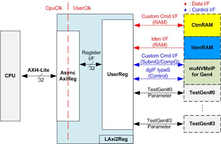
Figure 2‑11 CPU and peripherals hardware
LAxi2Reg consists of AsyncAxiReg and UserReg. AsyncAxiReg converts AXI4-Lite signals into a simple Register interface with a 32-bit data bus size, similar to the AXI4-Lite data bus size. It also includes asynchronous logic to handle clock domain crossing between the CpuClk and UserClk domains.
UserReg includes the register file of parameters and the status signals of other modules in the test system, including the CtmRAM, IdenRAM, muNVMe-IP, and TestGen. More details of AsyncAxiReg and UserReg are explained below.
2.3.1 AsyncAxiReg
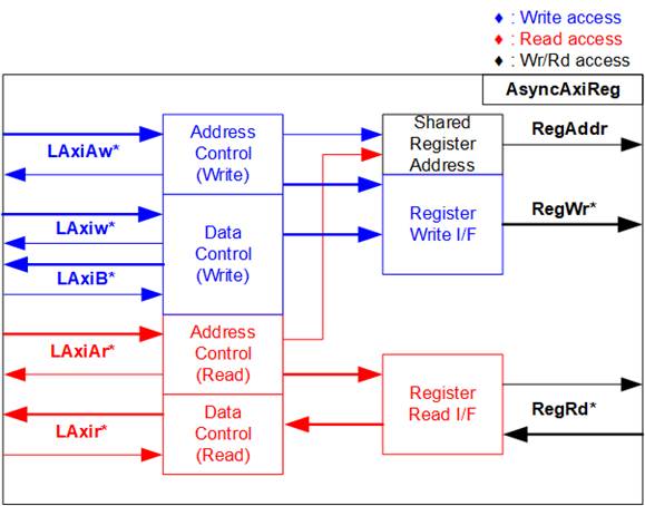
Figure 2‑12 AsyncAxiReg Interface
The signal on AXI4-Lite bus interface can be grouped into five categories, i.e., LAxiAw* (Write address channel), LAxiw* (Write data channel), LAxiB* (Write response channel), LAxiAr* (Read address channel), and LAxir* (Read data channel). More details to build Custom logic for AXI4-Lite bus can be found in the following document.
https://github.com/Architech-Silica/Designing-a-Custom-AXI-Slave-Peripheral/blob/master/
designing_a_custom_axi_slave_rev1.pdf
According to AXI4-Lite standard, the write channel and read channel operate independently for both control interface and data interfaces. Therefore, the logic within AsyncAxiReg to interface with AXI4-Lite bus is divided into four groups, i.e., Write control logic, Write data logic, Read control logic, and Read data logic, as shown in the left side of Figure 2‑12. The Write control I/F and Write data I/F of the AXI4-Lite bus are latched and transferred to become the Write register interface with clock domain crossing registers. Similarly, the Read control I/F of AXI4-Lite bus is latched and transferred to the Read register interface, while Read data is returned from Register interface to AXI4-Lite bus via clock domain crossing registers. In the Register interface, RegAddr is a shared signal for write and read access, so it loads the value from LAxiAw for write access or LAxiAr for read access.
The Register interface is compatible with single-port RAM interface for write transaction. The read transaction of the Register interface has been slightly modified from RAM interface by adding the RdReq and RdValid signals to control read latency time. The address of Register interface is shared for both write and read transactions, so user cannot write and read the register at the same time. The timing diagram of the Register interface is shown in Figure 2‑13.
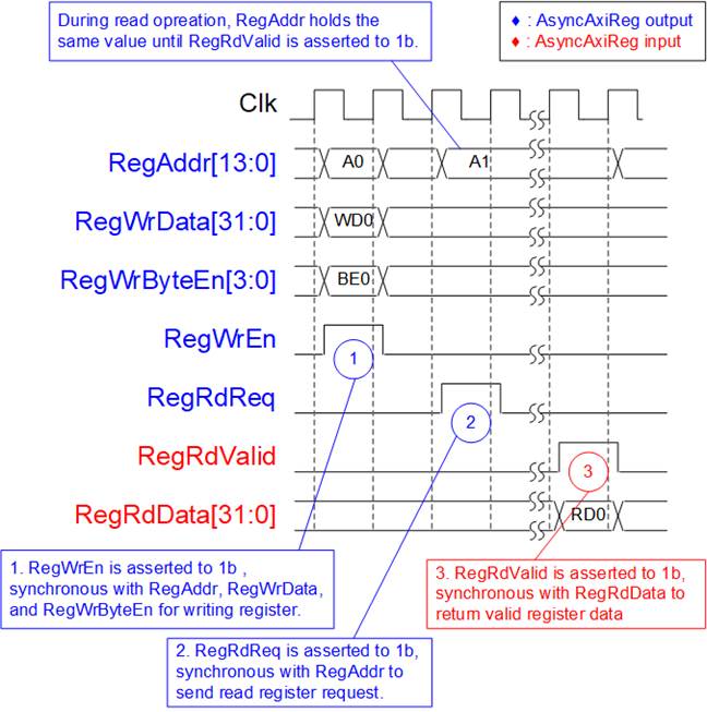
Figure 2‑13 Register interface timing diagram
1) Timing diagram to write register is similar to that of a single-port RAM. The RegWrEn signal is set to 1b, along with a valid RegAddr (Register address in 32-bit units), RegWrData (write data for the register), and RegWrByteEn (write byte enable). The byte enable consists of four bits that indicate the validity of the byte data. For example, bit[0], [1], [2], and [3] are set to 1b when RegWrData[7:0], [15:8], [23:16], and [31:24] are valid, respectively.
2) To read register, AsyncAxiReg sets the RegRdReq signal to 1b with a valid value for RegAddr. The 32-bit data is returned after the read request is received. The slave detects the RegRdReq signal being set to start the read transaction. In the read operation, the address value (RegAddr) remains unchanged until RegRdValid is set to 1b. The address can then be used to select the returned data using multiple layers of multiplexers.
3) The slave returns the read data on RegRdData bus by setting the RegRdValid signal to 1b. After that, AsyncAxiReg forwards the read value to the LAxir* interface.
2.3.2 UserReg
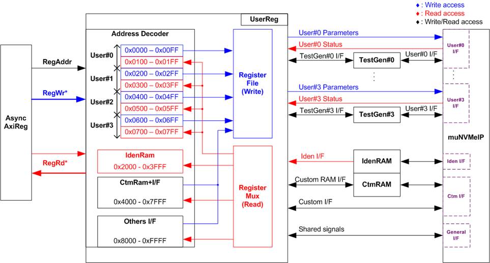
Figure 2‑14 UserReg Interface
The UserReg module consists of an Address decoder, a Register File, and a Register Mux. The Address decoder decodes the address requested by AsyncAxiReg and selects the active register for either write or read transactions. The assigned address range in UserReg is divided into eight areas, as shown in Figure 2‑14.
1) 0x0000 – 0x01FF: mapped to User#0 and TestGen#0
2) 0x0200 – 0x03FF: mapped to User#1 and TestGen#1
3) 0x0400 – 0x05FF: mapped to User#2 and TestGen#2
4) 0x0600 – 0x07FF: mapped to User#3 and TestGen#3
5) 0x2000 – 0x3FFF: mapped to read data from IdenRAM (read-only access).
6) 0x4000 – 0x5FFF: mapped to write/ read data with Custom command RAM interface (write and read access). However, the demo shows only read access by SMART command.
7) 0x6000 – 0x7FFF: mapped to Custom command interface
8) 0x8000 – 0xFFFF: mapped to other interfaces such as shared parameters for all Users, PCIe status, and IP version.
The Address decoder decodes the upper bits of RegAddr to select the active hardware (muNVMe-IP, TestGen#0-#3, IdenRAM, or CtmRAM). The Register File within UserReg has a 32-bit bus size, so the write byte enable (RegWrByteEn) is not used in the test system and the CPU uses 32-bit pointer to set the hardware register.
For reading a register, multi-level multiplexers (mux) select the data to return to CPU, by using the address. The lower bits of RegAddr are fed to the submodule to select the active data from each sub module. While the upper bits are used in UserReg to select the returned data from each submodule. The total latency time of read data is equal to three clock cycles, and RegRdValid is created by RegRdReq by asserting three D Flip-flops. More details of the address mapping within UserReg module are shown in Table 2‑1.
Table 2‑1 Register map defintion
|
Address |
Register Name |
Description |
|
Rd/Wr |
(Label in the “munvmeiptest.c”) |
|
|
0x0000 – 0x01FF: Signal Interface of User#0 (muNVMe-IP) and TestGen#0 |
||
|
0x0000 – 0x00FF: Control signals of User#0 and TestGen#0 (Write access only) |
||
|
BA+0x0000 |
User#0 Address (Low) Reg |
[31:0]: Input to be bit[31:0] of User#0 start address as 512-byte unit (U0Addr[31:0] of muNVMe-IP) |
|
(U0ADRL_INTREG) |
||
|
BA+0x0004 |
User#0 Address (High) Reg |
[15:0]: Input to be bit[47:32] of User#0 start address as 512-byte unit (U0Addr[47:32] of muNVMe-IP) |
|
(U0ADRH_INTREG) |
||
|
BA+0x0008 |
User#0 Length (Low) Reg |
[31:0]: Input to be bit[31:0] of User#0 transfer length as 512-byte unit (U0Len[31:0] of muNVMe-IP) |
|
(U0LENL_INTREG) |
||
|
BA+0x000C |
User#0 Length (High) Reg |
[15:0]: Input to be bit[47:32] of User#0 transfer length as 512-byte unit (U0Len[47:32] of muNVMe-IP) |
|
(U0LENH_INTREG) |
||
|
BA+0x0010 |
User#0 Command Reg |
[2:0]: Input to be User#0 command (U0Cmd of muNVMe-IP) 000b: Identify, 001b: Shutdown, 010b: Write SSD, 011b: Read SSD, 100b: SMART, 110b: Flush, 101b/111b: Reserved When this register is written, the command request is sent to muNVMe-IP via User#0 I/F to start the operation. |
|
(U0CMD_INTREG) |
||
|
BA+0x0014 |
User#0 Test Pattern Reg |
[2:0]: Select test pattern of TestGen#0 000b-Increment, 001b-Decrement, 010b-All 0, 011b-All 1, 100b-LFSR |
|
(U0PATTSEL_INTREG) |
||
|
BA+0x0018 |
User#0 Transfer Rate Reg |
[6:0]: Transfer Rate in percentage unit of TestGen#0. Valid from 1 – 100. For example, when this value=40, the maximum data rate is equal to 40% of 275 MHz x 256-bit (8.8 GB/s)=3520 MB/s. |
|
(U0TRNRATE_INTREG) |
||
|
0x0100 – 0x01FF: Status signals of User#0 and TestGen#0 (Read access only) |
||
|
BA+0x0100 |
User#0 Status Reg |
[0]: User#0 Busy of muNVMe-IP (0b: Idle,1b: Busy) [1]: U0Error of muNVMe-IP (0b: Normal,1b: Error) [2]: Data verification fail in TestGen#0 (0b: Normal,1b: Error) |
|
(U0STS_INTREG) |
||
|
BA+0x0104 |
User#0 Error Type Reg |
[31:0]: Mapped to U0ErrorType[31:0] of muNVMe-IP to show error status |
|
(U0ERRTYPE_INTREG) |
||
|
BA+0x0108 |
User#0 Completion Status Reg |
[15:0]: Mapped to U0AdmCompStatus[15:0] of muNVMe-IP [31:16]: Mapped to U0IOCompStatus[15:0] of muNVMe-IP |
|
(U0COMPSTS_INTREG) |
||
|
BA+0x0110 |
User#0 Test pin (Low) Reg |
[31:0]: Mapped to U0TestPin[31:0] of muNVMe-IP |
|
(U0TESTPINL_INTREG) |
||
|
BA+0x0114 |
User#0 Test pin (High) Reg |
[15:0]: Mapped to U0TestPin[47:32] of muNVMe-IP |
|
(U0TESTPINH_INTREG) |
||
|
BA+0x0140- BA+0x015F |
User#0 Expected value Word0-7 Reg |
256-bit of the expected data at the 1st failure data in TestGen#0 when operating Read command 0x0140: Bit[31:0], 0x0144: Bit[63:32], …, 0x015C: Bit[255:224] |
|
(U0EXPPATW0-W7_INTREG) |
||
|
BA+0x0160- BA+0x017F |
User#0 Read value Word0-3 Reg |
256-bit of the read data at the 1st failure data in TestGen#0 when operating Read command 0x0160: Bit[31:0], 0x0164: Bit[63:32], …, 0x017C: Bit[255:224] |
|
(U0RDPATW0-W7_INTREG) |
||
|
BA+0x0180 |
User#0 Data Failure Address(Low) Reg |
[31:0]: Bit[31:0] of the byte address of the 1st failure data in TestGen#0 when operating Read command |
|
(U0RDFAILNOL_INTREG) |
||
|
BA+0x0184 |
User#0 Data Failure Address(High) Reg |
[24:0]: Bit[56:32] of the byte address of the 1st failure data in TestGen#0 when operating Read command |
|
(U0RDFAILNOH_INTREG) |
||
|
BA+0x0188 |
User#0 Current test byte (Low) Reg |
[31:0]: Bit[31:0] of the current test data size in TestGen#0 module |
|
(U0CURTESTSIZEL_INTREG) |
||
|
BA+0x018C |
User#0 Current test byte (High) Reg |
[24:0]: Bit[56:32] of the current test data size of TestGen#0 module |
|
(U0CURTESTSIZEH_INTREG) |
||
|
Address |
Register Name |
Description |
|
Rd/Wr |
(Label in the “munvmeiptest.c”) |
|
|
0x0200 – 0x07FF: Signal Interface of User#1-#3 (muNVMe-IP) and TestGen#1-#3 |
||
|
0x0200 – 0x02FF: Control signals of User#1 and TestGen#1 (Write access only) |
||
|
BA+0x0200- BA+0x021B |
Control signals of User#1/TestGen#1 |
Similar to 0x0000 – 0x001B which are the registers of User#0 and TestGen#0, these are mapped to User#1 and TestGen#1 instead. However, U1CMD_INTREG can be assigned by two values for two commands – 010b: Write SSD and 011b: Read SSD. |
|
(U1ADRL_INTREG – U1TRNRATE_INTREG) |
||
|
0x0300 – 0x03FF: Status signals of User#1 and TestGen#1 (Read access only) |
||
|
BA+0x0300- BA+0x038F |
Status signals of User#1/TestGen#1 |
Similar to 0x0100 – 0x018F which are the registers of User#0 and TestGen#0, these are mapped to User#1 and TestGen#1 instead. However, there are some status signals that are available for User#0 only and not available for other Users, i.e., U0COMPSTS_INTREG[15:0], U0TESTPINL_INTREG[31:16], and U0TESTPINH_INTREG[15:0]. These registers are reserved for other Users. |
|
(U1STS_INTREG – U1CURTESTSIZEH_INTREG) |
||
|
0x0400 – 0x07FF: Signal interface of User#2-#3 and TestGen#2-#3 |
||
|
BA+0x0400- BA+0x078F |
(U2ADRL_INTREG – U3CURTESTSIZEH_INTREG) |
Similar to 0x0200 – 0x038F which are the registers of User#1 and TestGen#1, these are mapped to User#2-#3 and TestGen#2-#3. 0x400 – 0x58F: User#2 and TestGen#2 0x600 – 0x78F: User#3 and TestGen#3 |
|
0x2000 – 0x3FFF: IdenRAM (Read access only) |
||
|
BA+0x2000- BA+0x2FFF |
Identify Controller Data |
4Kbyte Identify Controller Data Structure |
|
(IDENCTRL_CHARREG) |
||
|
BA+0x3000-BA+0x3FFF |
Identify Namespace Data |
4Kbyte Identify Namespace Data Structure |
|
(IDENNAME_CHARREG) |
||
|
0x4000 – 0x5FFF: CtmRAM (Write/Read access) |
||
|
BA+0x4000-BA+0x5FFF |
Custom command Ram |
Connect to 8Kbyte CtmRAM interface for storing 512-byte data that is output from SMART Command. |
|
(CTMRAM_CHARREG) |
||
|
0x6000 – 0x7FFF: Custom Command Interface |
||
|
BA+0x6000- BA+0x603F |
Custom Submission Queue Reg |
[31:0]: Submission queue entry of SMART and Flush command. Input to be CtmSubmDW0-DW15 of muNVMe-IP. 0x6000: DW0, 0x6004: DW1, …, 0x603C: DW15 |
|
Wr |
(CTMSUBMQ_STRUCT) |
|
|
BA+0x6100-BA+0x610F |
Custom Completion Queue Reg |
[31:0]: CtmCompDW0-DW3 output from muNVMe-IP. 0x6100: DW0, 0x6104: DW1, …, 0x610C: DW3 |
|
Rd |
(CTMCOMPQ_STRUCT) |
|
|
Address |
Register Name |
Description |
|
Rd/Wr |
(Label in the “munvmeiptest.c”) |
|
|
0x8000 – 0xFFFF: Other Interfaces |
||
|
BA+0x8000 |
NVMe Timeout Reg |
[31:0]: Mapped to TimeOutSet[31:0] of muNVMe-IP |
|
Wr |
(NVMTIMEOUT_INTREG) |
|
|
BA+0x8100 |
PCIe Status Reg |
[0]: PCIe linkup status from PCIe hard IP (0b: No linkup,1b: linkup) [3:2]: Two lower bits to show PCIe link speed of PCIe hard IP. MSB is bit[16]. (000b: Not linkup, 001b: PCIe Gen1, 010b: PCIe Gen2, 011b: PCIe Gen3, 111b: PCIe Gen4) [7:4]: PCIe link width status from PCIe hard IP (0001b: 1-lane, 0010b: 2-lane, 0100b: 4-lane, 1000b: 8-lane) [13:8]: Current LTSSM State of PCIe hard IP. Please see more details of LTSSM value in Integrated Block for PCIe datasheet [16]: The upper bit to show PCIe link speed of PCIe hard IP. Two lower bits are bit[3:2]. |
|
Rd |
(PCIESTS_INTREG) |
|
|
BA+0x8110 |
NVMe CAP Reg |
[31:0]: Mapped to NVMeCAPReg[31:0] of muNVMe-IP |
|
Rd |
(NVMCAP_INTREG) |
|
|
BA+0x8120 |
Total disk size (Low) Reg |
[31:0]: Mapped to LBASize[31:0] of muNVMe-IP |
|
Rd |
(LBASIZEL_INTREG) |
|
|
BA+0x8124 |
Total disk size (High) Reg |
[15:0]: Mapped to LBASize[47:32] of muNVMe-IP [31]: Mapped to LBAMode of muNVMe-IP |
|
Rd |
(LBASIZEH_INTREG) |
|
|
BA+0x8200 |
IP Version Reg |
[31:0]: Mapped to IPVersion[31:0] of muNVMe-IP |
|
Rd |
(IPVERSION_INTREG) |
|
3 CPU Firmware
3.1 Test firmware (munvmeiptest.c)
The CPU follows these steps upon system startup to complete the initialization process.
1) Initialize UART and Timer settings.
2) Wait for the PCIe connection to become active (PCIESTS_INTREG[0]=1b).
3) Wait for muNVMe-IP to finish its own initialization process (U0-U3STS_INTREG[0]=0b). If any errors occur during this process, an error message will be displayed, and the initialization will be halted.
4) Display the status of the PCIe link, including information about the number of lanes and the speed, by reading PCIESTS_INTREG[16:2].
5) Display the main menu with five options for executing six commands of muNVMe-IP. These commands are Identify, Write, Read, SMART, Flush, and Shutdown.
Further details regarding the sequence of each command in the CPU firmware are provided in the following sections.
3.1.1 Identify Command
The sequence for the firmware when the Identify command is selected by User#0 I/F is as follows.
1) Set U0CMD_INTREG=000b to send the Identify command request to User#0 I/F of muNVMe-IP. The busy flag of User#0 I/F (U0STS_INTREG[0]) will then changes from 0b to 1b.
2) The CPU will wait until the operation is completed or an error is detected by monitoring U0STS_INTREG[1:0].
· If bit[0] is de-asserted to 0b after the operation is finished, the data of Identify command returned by muNVMe-IP will be stored in IdenRAM.
· If bit[1] is asserted to 1b, indicating an error. the error message will be displayed on the console with details decoded from U0ERRTYPE_INTREG[31:0]. The process will then stop.
3) After the busy flag (U0STS_INTREG[0]) is de-asserted to 0b, the CPU will display some information decoded from IdenRAM (IDENCTRL_CHARREG), such as the SSD model name and the information from muNVMe-IP output, such as SSD capacity and LBA unit size (LBASIZEH/L_INTREG).
3.1.2 Write/Read Command
When the user selects the Write/Read command that can be requested from all users (User#0 – User#3 I/F), the firmware follows the following sequence.
1) Receive four sets of parameters to assign to each user interface such as the command (enable or not), the start address, transfer length, test pattern, and transfer rate from the console. If any inputs are invalid, the operation will be cancelled.
Note: If LBA unit size = 4 Kbyte, start address and transfer length must be aligned to 8.
2) After obtaining all the inputs, set them to U0-U3ADRL/H_INTREG, U0-U3LENL/H_INTREG, U0-U3PATTSEL_INTREG, and U0-U3TRNRATE_INTREG.
3) Set U0-U3CMD_INTREG[2:0] to 010b for the Write command or 011b for the Read command. This sends the command request to the corresponding User I/F. Once the command is issued, the busy flag of the active user (U0-U3STS_INTREG[0]) will change from 0b to 1b.
4) The CPU waits until the operation is completed or an error (excluding verification error) is detected by monitoring U0-U3STS_INTREG[2:0].
· Bit[0] will be de-asserted to 0b when the User#0-#3 is complete.
· Bit[1] will be asserted when an error is detected in User#0-#3. In this case, the error message will be displayed on the console to show the error details, and the process is halted.
· Bit[2] will be asserted when data verification fails in User#0-#3. Afterward, the verification error message is displayed on the console, but the CPU will continue to run until the operation is complete or the user inputs any key to cancel the operation.
During the command execution, the current transfer size of the active user, read from U0-U3CURTESTSIZEL/H_INTREG, will be displayed every second.
5) Once the busy flag (U0-U3STS_INTREG[0]) is de-asserted to 0b, CPU will display the test result of the active user on the console, including the total time usage, total transfer size, and transfer speed.
3.1.3 SMART Command
This command can be requested by User#0 I/F. The sequence of the firmware when user selects SMART command is below.
1) The 16-Dword of the Submission queue entry (CTMSUBMQ_STRUCT) is set to the SMART command value.
2) Set U0CMD_INTREG[2:0]=100b to send SMART command request to User#0 I/F of muNVMe-IP. The busy flag of User#0 I/F (U0STS_INTREG[0]) will then change from 0b to 1b.
3) The CPU will wait until the operation is completed or an error is detected by monitoring U0STS_INTREG[1:0].
· If bit[0] is de-asserted to 0b after the operation is finished, the data of SMART command returned by muNVMe-IP will be stored in CtmRAM.
· If bit[1] is asserted to 1b, indicating an error, the error message will be displayed on the console with details decoded U0ERRTYPE_INTREG[31:0]. The process will then stop.
4) After the busy flag (U0STS_INTREG[0]) is de-asserted to 0b, the CPU will display information decoded from CtmRAM (CTMRAM_CHARREG), such as Remaining Life, Percentage Used, Temperature, Total Data Read, Total Data Written, Power On Cycles, Power On Hours, and Number of Unsafe Shutdown.
For more information on the SMART log, refer to the NVM Express Specification.
https://nvmexpress.org/resources/specifications/
3.1.4 Flush Command
This command can be requested by User#0 I/F. The sequence of the firmware when user selects Flush command is below.
1) The 16-Dword of the Submission queue entry (CTMSUBMQ_STRUCT) is set to the Flush command value.
2) Set U0CMD_INTREG[2:0]=110b to send Flush command request to User#0 I/F of muNVMe-IP. The busy flag of User#0 I/F (U0STS_INTREG[0]) will then change from 0b to 1b.
3) The CPU will wait until the operation is completed or an error is detected by monitoring U0STS_INTREG[1:0].
· If bit[0] is de-asserted to 0b after the operation is finished. The CPU will then return to the main menu.
· If bit[1] is asserted to 1b, indicating an error, the error message will be displayed on the console with details decoded U0ERRTYPE_INTREG[31:0]. The process will then stop.
3.1.5 Shutdown Command
This command can be requested by User#0 I/F. The sequence of the firmware when user selects Shutdown command is below.
1) Set U0CMD_INTREG[2:0]=001b to send the Shutdown command request to User#0 I/F of muNVMe-IP. The busy flag of User#0 I/F (U0STS_INTREG[0]) will then change from 0b to 1b.
2) The CPU will wait until the operation is completed or an error is detected by monitoring U0STS_INTREG[1:0].
· If bit[0] is de-asserted to 0b after the operation is finished, the CPU will then proceed to the next step.
· If bit[1] is asserted to 1b, indicating an error, the error message will be displayed on the console with details decoded U0ERRTYPE_INTREG[31:0].The process will then stop.
3) After Shutdown command completes, both the SSD and muNVMe-IP will become inactive and the CPU will be unable to receive any new commands from the user. To continue testing, the user must power off and power on the system.
3.2 Function list in Test firmware
|
int exec_ctm(unsigned int user_cmd) |
|
|
Parameters |
user_cmd: 4-SMART command, 6-Flush command |
|
Return value |
0: No error, -1: Some errors are found in the muNVMe-IP |
|
Description |
Execute SMART command as outlined in section 3.1.3 (SMART Command), or execute Flush command as outlined in section 3.1.4 (Flush Command). |
|
unsigned long long get_cursize(unsigned int user) |
|
|
Parameters |
user: 0-3 for User#0-#3, respectively |
|
Return value |
Read value of U0-3CURTESTSIZEH/L_INTREG |
|
Description |
The value of U0-3CURTESTSIZEH/L_INTREG is read and converted to byte units before being returned as the result of the function. |
|
int get_param(userin_struct* userin) |
|
|
Parameters |
userin: Five inputs from user, i.e., command, start address, total length in 512-byte unit, test pattern, and transfer rate |
|
Return value |
0: Valid input, -1: Invalid input |
|
Description |
Receive the input parameters from the user and verify the value. When the input is invalid, the function returns -1. Otherwise, all inputs are updated to userin parameter. |
|
void iden_dev(void) |
|
|
Parameters |
None |
|
Return value |
None |
|
Description |
Execute Identify command as outlined in section 3.1.1 (Identify Command). |
|
void print_space(unsigned long long size_input) |
|
|
Parameters |
size_input: test size to display on the console |
|
Return value |
None |
|
Description |
Calculate the number of digits and spaces required to properly align and display the size_input on the console. |
|
int setctm_flush(void) |
|
|
Parameters |
None |
|
Return value |
0: No error, -1: Some errors are found in the muNVMe-IP |
|
Description |
Set Flush command to CTMSUBMQ_STRUCT and call exec_ctm function to execute Flush command. |
|
int setctm_smart(void) |
|
|
Parameters |
None |
|
Return value |
0: No error, -1: Some errors are found in the muNVMe -IP |
|
Description |
Set SMART command to CTMSUBMQ_STRUCT and call exec_ctm function to execute SMART command. Finally, decode and display SMART information on the console |
|
void show_error(unsigned int user) |
|
|
Parameters |
user: 0-3 for User#0-#3, respectively |
|
Return value |
None |
|
Description |
Read U0-U3ERRTYPE, decode the error flag, and display the corresponding error message. Also, call show_pciestat function to check the hardware’s debug signal. |
|
void show_pciestat(void) |
|
|
Parameters |
None |
|
Return value |
None |
|
Description |
Read PCIESTS_INTREG until the read value from two read times is stable. After that, display the read value on the console. Also, debug signals are read from U0-U3TESTPINL/H_INTREG. |
|
void show_result(unsigned int user, unsigned int cmd, unsigned int timeuseh, unsigned int timeusel) |
|
|
Parameters |
user: 0-3 for User#0-#3, respectively cmd: 0-Write, 1-Read timeuseh, timeusel: 64-bit read value of timer |
|
Return value |
None |
|
Description |
Print user channel, command, and total size by calling get_cursize and show_size function. After that, calculate total time usage from timeuseh and timeusel and then display in usec, msec, or sec unit. Finally, transfer performance is calculated and displayed in MB/s unit. |
|
void show_size(unsigned long long size_input) |
|
|
Parameters |
size_input: transfer size to display on the console |
|
Return value |
None |
|
Description |
Calculate and display the input value in Mbyte, Gbyte, or Tbyte unit |
|
void show_smart_hex16byte(volatile unsigned char *char_ptr) |
|
|
Parameters |
*char_ptr: Pointer of 16-byte SMART data |
|
Return value |
None |
|
Description |
Display 16-byte SMART data as hexadecimal unit |
|
void show_smart_int8byte(volatile unsigned char *char_ptr) |
|
|
Parameters |
*char_ptr: Pointer of 8-byte SMART data |
|
Return value |
None |
|
Description |
When the input value is less than 4 billion (32-bit), the 8-byte SMART data is displayed in decimal units. If the input value exceeds this limit, an overflow message is displayed. |
|
void show_smart_size8byte(volatile unsigned char *char_ptr) |
|
|
Parameters |
*char_ptr: Pointer of 8-byte SMART data |
|
Return value |
None |
|
Description |
Display 8-byte SMART data as GB or TB unit. When the input value is more than limit (500 PB), the overflow message is displayed instead. |
|
void show_vererr(unsigned int user) |
|
|
Parameters |
user: 0-3-User#0-#3, respectively |
|
Return value |
None |
|
Description |
Read U0-U3RDFAILNOL/H_INTREG (error byte address), U0-U3EXPPATW0-W3_INTREG (expected value), and U0-U3RDPATW0-W3_INTREG (read value) to display verification error details on the console. |
|
void shutdown_dev(void) |
|
|
Parameters |
None |
|
Return value |
None |
|
Description |
Execute Shutdown command as outlined in section 3.1.5 (Shutdown Command) |
|
int wrrd_dev(void) |
|
|
Parameters |
None |
|
Return value |
0: No error, -1: Receive invalid input |
|
Description |
Execute Write command or Read command as outlined in section 3.1.2 (Write/Read Command). “show_result” function is called to calculate and display transfer performance of the Write/Read command. |
4 Example Test Result
Figure 4‑1 and Figure 4‑2 show the test results obtained from running the demo system with a single user and four users, respectively. Two figures represent two different test environments. In Figure 4‑1, the results are obtained using a 2 TB Addlink S95 SSD, a transfer size of 32 GB per user, and an all-zero test pattern, which demonstrates optimal performance. On the other hand, Figure 4‑2 shows the results achieved with an 800 GB Intel P5800X SSD, a transfer size of 32 GB per user, and an LFSR test pattern, which exhibits good performance under various conditions.
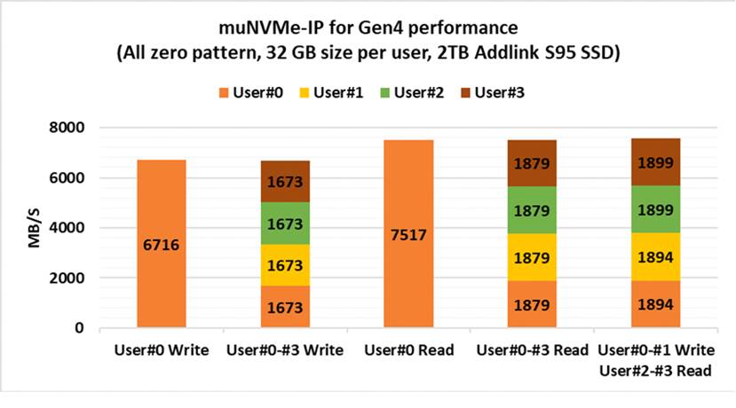
Figure 4‑1 Test Performance when using 2 TB Addlink S95 by 32 GB Zero pattern
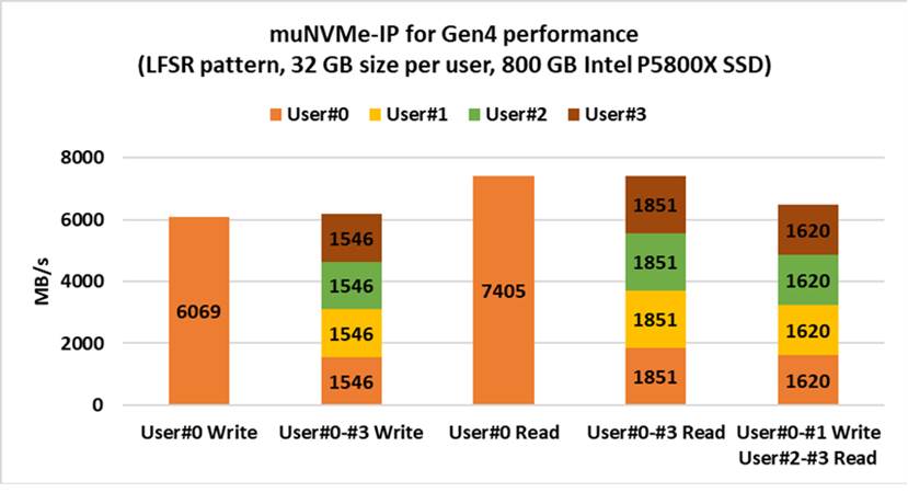
Figure 4‑2 Test Performance when using 800GB Intel P5800X by 32 GB LFSR pattern
As shown in Figure 4‑1 and Figure 4‑2, the total performance of User#0 Write and User#0-#3 Write is equivalent. Similarly, the total performance of User#0 Read and User#0-#3 Read also match. The performance of each user during the User#0-#3 Write/Read operation (1673 MB/s or 1879 MB/s) is approximately one-fourth of the performance achieved during User#0 Write/Read (6716 MB/s or 7517 MB/s). Furthermore, the mixed Write-Read command (User#0-#1 Write, User#2-#3 Read) demonstrates good load balancing for both test conditions. However, when the test conditions change, such as using larger transfer size and random test pattern, the performance of most SSDs tends to decrease.
Typically, SSD incorporate caching mechanisms that deliver good performance for Write/Read commands until the cache is full. Additionally, certain SSDs employ algorithms optimized for processing data using all-zero pattern, rather than random pattern, to achieve better performance. However, there are exceptions, such as the 800 GB Intel P5800X, which exhibits consistent and good performance when utilizing the LFSR pattern and large transfer sizes, as shown in Figure 4‑2.
5 Revision History
|
Revision |
Date |
Description |
|
1.0 |
2-Jun-23 |
Initial Release |
Copyright: 2023 Design Gateway Co,Ltd.