NVMe-IP with PCIe Gen3 Soft IP reference design manual
Rev1.0 28-Jun-23
1 NVMe
NVM Express (NVMe) defines the interface for the host controller to access solid state drives (SSD) by PCI Express. NVM Express optimizes the process to issue command and completion by using only two registers (Command issue and Command completion). Besides, NVMe supports parallel operation by supporting up to 64K commands within single queue. 64K command entries improves transfer performance for both sequential and random access.
In PCIe SSD market, two standards are used, i.e. AHCI and NVMe. AHCI is the older standard to provide the interface for SATA hard disk drive while NVMe is optimized for non-volatile memory like SSD. The comparison between both AHCI and NVMe protocol in more details is described in “A Comparison of NVMe and AHCI” document.
https://sata-io.org/system/files/member-downloads/NVMe%20and%20AHCI_%20_long_.pdf
The example of NVMe storage device is shown in http://www.nvmexpress.org/products/.

Figure 1‑1 NVMe protocol layer
DG NVMe-IP is the NVMe host controller to access NVMe SSD without using CPU and external memory, as shown in the left side of Figure 1‑1. The low-level protocol of NVMe-IP system uses Avalon-ST PCIe Hard IP, so the maximum SSD for connecting to FPGA is limited by the number of PCIe Hard IP. Comparing to the right side of Figure 1‑1, NVMeG3-IP designs most layers by pure-hardwired logic. Only a part of Physical layer is designed by using Native PHY IP which implemented by Intel Transceiver with the logic. So, the maximum SSD for connecting to FPGA is limited by the number of Transceiver instead of PCIe Hard IP. However, using NVMeG3-IP uses much logic resource to implement many layers comparing with NVMe-IP. It is recommended to use NVMe-IP firstly if the FPGA can fit with the system requirement. Otherwise, NVMeG3-IP must be used instead to support the big system which needs to connect many NVMe SSDs. The user interface of NVMe-IP and NVMeG3-IP is similar.
2 Hardware overview

Figure 2‑1 NVMeG3-IP demo hardware
User interface of NVMeG3-IP and NVMe-IP are similar, so all modules of user interface such as TestGen and CPU system in NVMeG3IPTest are similar to NVMe-IP reference design. The different module is PCIe interface which using Native PHY IP instead of Avalon-ST PCIe hard IP, as shown in Figure 2‑1.
This document describes only the modification point of NVMeG3-IP reference design from NVMe-IP reference design. Please see more details of the user interface in NVMe-IP reference design document, provided on our website.
https://dgway.com/products/IP/NVMe-IP/dg_nvmeip_refdesign_intel_en.pdf
In NVMe-IP reference design document, it describes the details of the logic design with timing diagram of TestGen, Avl2Reg, RAM, and FIFO.
In NVMeG3-IP reference design, there are the status and test signals which is the output of MAC layer within NVMeG3-IP, i.e. MACTestPin and MACStatus. So, these signals are mapped to the CPU for displaying the debug message when some problems are found. UserReg within Avl2Reg is slightly modified to read these signals by CPU, as shown in Table 2‑1.
Table 2‑1 Register Map
|
Address |
Register Name |
Description |
|
Rd/Wr |
(Label in the “nvmeg3iptest.c”) |
|
|
0x0000 – 0x00FF: Control signals of NVMeG3-IP and TestGen (Write access only) |
||
|
BA+0x0000 |
User Address (Low) Reg |
[31:0]: Input to be start address as 512-byte unit (UserAddr[31:0] of dgIF typeS) |
|
(USRADRL_REG) |
||
|
BA+0x0004 |
User Address (High) Reg |
[15:0]: Input to be start address as 512-byte unit (UserAddr[47:32] of dgIF typeS) |
|
(USRADRH_REG) |
||
|
BA+0x0008 |
User Length (Low) Reg |
[31:0]: Input to be transfer length as 512-byte unit (UserLen[31:0] of dgIF typeS) |
|
(USRLENL_REG) |
||
|
BA+0x000C |
User Length (High) Reg |
[15:0]: Input to be transfer length as 512-byte unit (UserLen[47:32] of dgIF typeS) |
|
(USRLENH_REG) |
||
|
BA+0x0010 |
User Command Reg |
[2:0]: Input to be user command (UserCmd of dgIF typeS for NVMeG3-IP) “000”: Identify, “001”: Shutdown, “010”: Write SSD, “011”: Read SSD, “100”: SMART, “110”: Flush, “101”/”111”: Reserved When this register is written, the command request is sent to NVMeG3-IP to start the operation. |
|
(USRCMD_REG) |
||
|
BA+0x0014 |
Test Pattern Reg |
[2:0]: Select test pattern “000”-Increment, “001”-Decrement, “010”-All 0, “011”-All 1, “100”-LFSR |
|
(PATTSEL_REG) |
||
|
BA+0x0020 |
NVMe Timeout Reg |
[31:0]: Timeout value of NVMeG3-IP (TimeOutSet[31:0] of NVMeG3-IP) |
|
(NVMTIMEOUT_REG) |
||
|
0x0100 – 0x01FF: Status signals of NVMeG3-IP and TestGen (Read access only) |
||
|
BA+0x0100 |
User Status Reg |
[0]: UserBusy of dgIF typeS (‘0’: Idle, ‘1’: Busy) [1]: UserError of dgIF typeS (‘0’: Normal, ‘1’: Error) [2]: Data verification fail (‘0’: Normal, ‘1’: Error) |
|
(USRSTS_REG) |
||
|
BA+0x0104 |
Total disk size (Low) Reg |
[31:0]: LBASize0[31:0] output from NVMeG3-IP
|
|
(LBASIZEL_REG) |
||
|
BA+0x0108 |
Total disk size (High) Reg |
[15:0]: LBASize0[47:32] output from NVMeG3-IP [31]: LBAMode output from NVMeG3-IP |
|
(LBASIZEH_REG) |
||
|
BA+0x010C |
User Error Type Reg |
[31:0]: User error status (UserErrorType[31:0] of dgIF typeS) |
|
(USRERRTYPE_REG) |
||
|
BA+0x0110 |
PCIe Status Reg |
[7:0]: Unused for NVMeG3-IP [15:8]: MACStatus output from NVMeG3-IP |
|
(PCISTS_REG) |
||
|
BA+0x0114 |
Completion Status Reg |
[15:0]: Status from Admin completion (AdmCompStatus[15:0] of NVMeG3-IP) [31:16]: Status from I/O completion (IOCompStatus[15:0] of NVMeG3-IP) |
|
(COMPSTS_REG) |
||
|
BA+0x0118 |
NVMe CAP Reg |
[31:0]: NVMeCAPReg[31:0] output from NVMeG3-IP |
|
(NVMCAP_REG) |
||
|
BA+0x0120 |
NVMe Test pin Reg |
[31:0]: TestPin[31:0] output from NVMeG3-IP |
|
(NVMTESTPIN_REG) |
||
|
BA+0x0124 |
MAC Test pin (Low) Reg |
[31:0]: MACTestPin[31:0] output from NVMeG3-IP |
|
(MACTESTPINL_REG) |
||
|
BA+0x0128 |
MAC Test pin (High) Reg |
[31:0]: MACTestPin[63:0] output from NVMeG3-IP |
|
(MACTESTPINH_REG) |
||
|
Address |
Register Name |
Description |
|
Rd/Wr |
(Label in the “nvmeg3iptest.c”) |
|
|
0x0100 – 0x01FF: Status signals of NVMeG3-IP and TestGen (Read access only) |
||
|
BA+0x0130 |
Expected value Word0 Reg |
[31:0]: Bit[31:0] of the expected data at the 1st failure data in Read command |
|
(EXPPATW0_REG) |
||
|
BA+0x0134 |
Expected value Word1 Reg |
[31:0]: Bit[63:32] of the expected data at the 1st failure data in Read command |
|
(EXPPATW1_REG) |
||
|
BA+0x0138 |
Expected value Word2 Reg |
[31:0]: Bit[95:64] of the expected data at the 1st failure data in Read command |
|
(EXPPATW2_REG) |
||
|
BA+0x013C |
Expected value Word3 Reg |
[31:0]: Bit[127:96] of the expected data at the 1st failure data in Read command |
|
(EXPPATW3_REG) |
||
|
BA+0x0140 |
Read value Word0 Reg |
[31:0]: Bit[31:0] of the read data at the 1st failure data in Read command |
|
(RDPATW0_REG) |
||
|
BA+0x0144 |
Read value Word1 Reg |
[31:0]: Bit[63:32] of the read data at the 1st failure data in Read command |
|
(RDPATW1_REG) |
||
|
BA+0x0148 |
Read value Word2 Reg |
[31:0]: Bit[95:64] of the read data at the 1st failure data in Read command |
|
(RDPATW2_REG) |
||
|
BA+0x014C |
Read value Word3 Reg |
[31:0]: Bit[127:96] of the read data at the 1st failure data in Read command |
|
(RDPATW3_REG) |
||
|
BA+0x0150 |
Data Failure Address(Low) Reg |
[31:0]: Bit[31:0] of the byte address of the 1st failure data in Read command |
|
(RDFAILNOL_REG) |
||
|
BA+0x0154 |
Data Failure Address(High) Reg |
[24:0]: Bit[56:32] of the byte address of the 1st failure data in Read command |
|
(RDFAILNOH_REG) |
||
|
BA+0x0158 |
Current test byte (Low) Reg |
[31:0]: Bit[31:0] of the current test data size in TestGen module |
|
(CURTESTSIZEL_REG) |
||
|
BA+0x015C |
Current test byte (High) Reg |
[24:0]: Bit[56:32] of the current test data size of TestGen module |
|
(CURTESTSIZEH_REG) |
||
|
Other interfaces (Custom command of NVMeG3-IP, IdenRAM, and Custom RAM) |
||
|
BA+0x0200-BA+0x023F |
Custom Submission Queue Reg |
[31:0]: Submission queue entry of SMART and Flush command. Input to be CtmSubmDW0-DW15 of NVMeG3-IP. 0x200: DW0, 0x204: DW1, …, 0x23C: DW15 |
|
Wr |
(CTMSUBMQ_REG) |
|
|
BA+0x0300-BA+0x030F |
Custom Completion Queue Reg |
[31:0]: CtmCompDW0-DW3 output from NVMeG3-IP. 0x300: DW0, 0x304: DW1, …, 0x30C: DW3 |
|
Rd |
(CTMCOMPQ_REG) |
|
|
BA+0x0800 |
IP Version Reg |
[31:0]: IP version number (IPVersion[31:0] of NVMeG3-IP) |
|
Rd |
(IPVERSION_REG) |
|
|
BA+0x2000-BA+0x2FFF |
Identify Controller Data
|
4Kbyte Identify Controller Data Structure |
|
Rd |
(IDENCTRL_REG) |
|
|
BA+0x3000-BA+0x3FFF |
Identify Namespace Data
|
4Kbyte Identify Namespace Data Structure |
|
Rd |
(IDENNAME_REG) |
|
|
BA+0x4000-BA+0x5FFF |
Custom command Ram
|
Connect to 8K byte CtmRAM interface. Used to store 512-byte data output from SMART Command. |
|
Wr/Rd |
(CTMRAM_REG) |
|
3 CPU Firmware
CPU Firmware on NVMeG3-IP reference design is slightly modified from NVMe-IP reference design in PCIe initialization sequence. The step to check PCIe link up signal is removed in NVMeG3-IP. After reset sequence is finished, the IP starts the initialization process by running the following steps.
1) CPU initializes UART and Timer parameters.
2) CPU waits until IP completes PCIe and NVMe initialization process by monitoring IP busy flag (USRSTS_REG[0]=’0’). When some errors are found, the process stops and displays the error message.
3) CPU displays the main menu. There are six menus for running six commands, i.e. Identify, Write, Read, SMART, Flush, and Shutdown.
The details of CPU firmware to operate all commands are similar to the sequence described in NVMe-IP reference design which are described in NVMe-IP reference design document.
4 Example Test Result
The example test result when running demo system by using 512 GB Samsung 970 Pro is shown in Figure 4‑1.
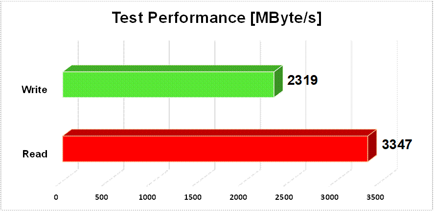
Figure 4‑1 Test Performance of NVMeG3-IP demo by using Samsung 970 Pro SSD
By using PCIe Gen3 on Arria10 GX board, write performance is about 2300 Mbyte/sec and read performance is about 3350 Mbyte/sec.
5 Revision History
|
Revision |
Date |
Description |
|
1.0 |
30-Apr-20 |
Initial Release |
Copyright: 2020 Design Gateway Co,Ltd.