FPGA Setup for NVMe-IP for Gen5 demo
This document describes the process of configuring an FPGA and setting up the environment to run the NVMe IP for Gen5 series demo with NVMe SSDs on an FPGA development board. These demos enable direct access to NVMe SSDs through a PCIe adapter board. The user can control the test operation through the NiosII command shell.
1 Environment Requirement
To run the demo on the FPGA development board, the following environment must be prepared.
1) Supported FPGA Development board: Intel Agilex 7 FPGA I-series Development Kit.
2) A PC with Quartus Prime programmer and NiosII command shell software installed.
3) The PCIe adapter board (AB19-M2PCI), provided by Design Gateway
https://dgway.com/ABseries_E.html
4) An Intel power adapter for the FPGA board
5) An ATX power supply for the AB19-M2PCI adapter board
6) One, two, or four NVMe Gen5 SSDs connected to the PCIe adapter board
7) A micro USB cable for FPGA programming and NiosII command shell, connecting the FPGA board to the PC.
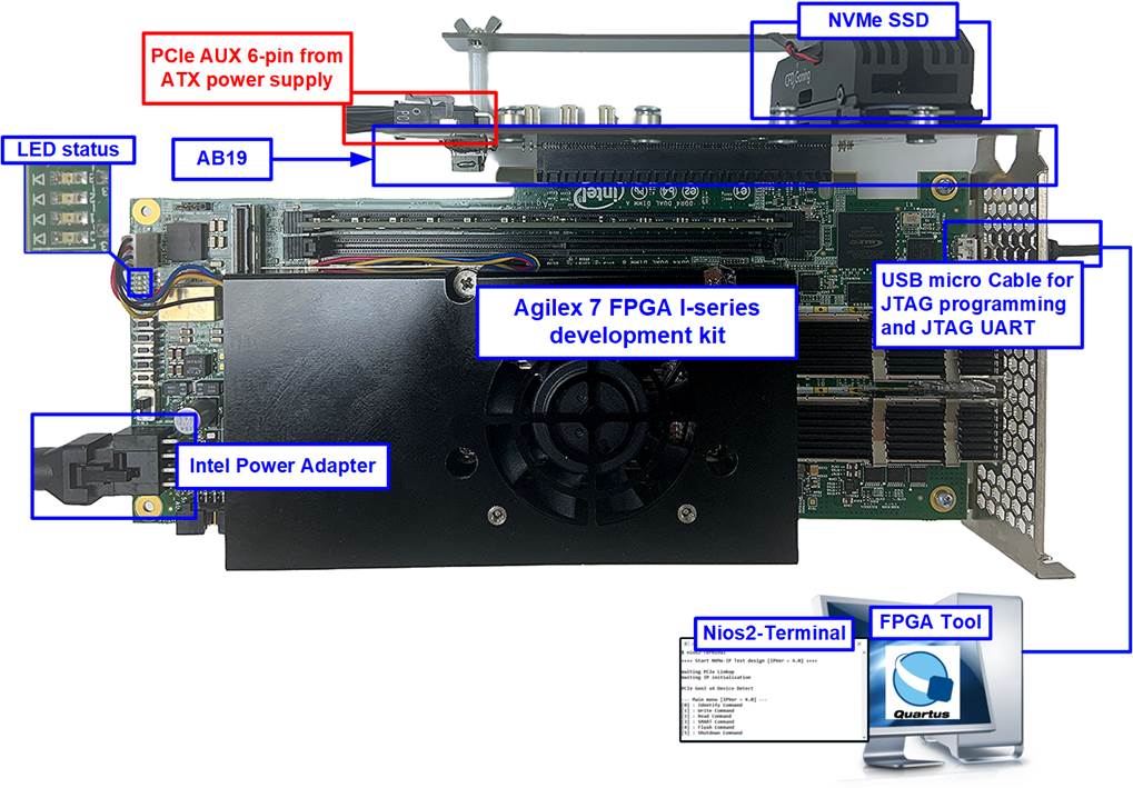
Figure 1‑1 NVMe-IP Standard demo setup on Intel Agilex 7 FPGA I-series Development kit
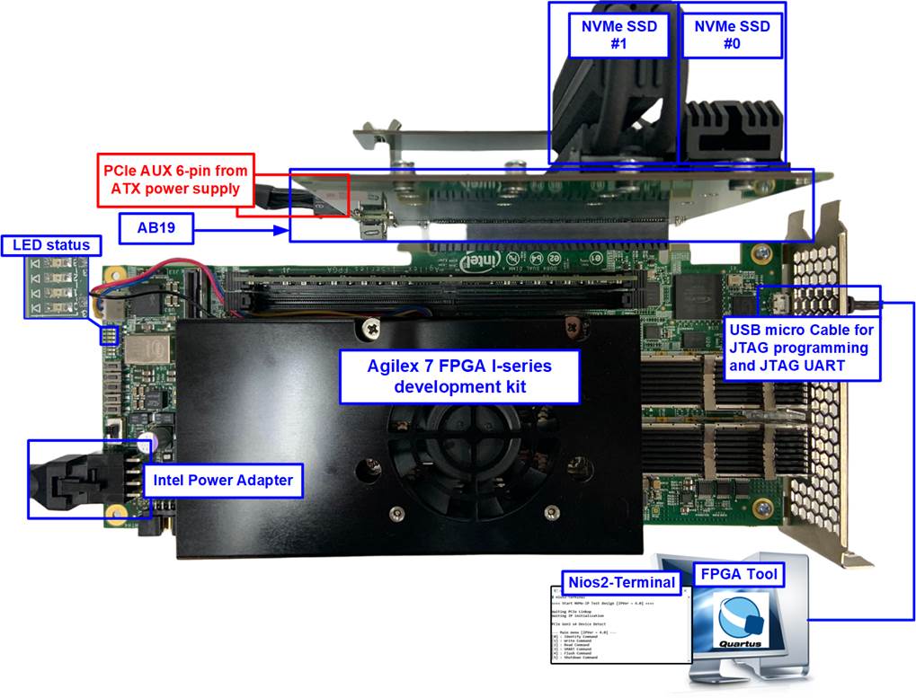
Figure 1‑2 NVMe-IP 2-ch RAID0 demo setup on Intel Agilex 7 FPGA I-series Development kit
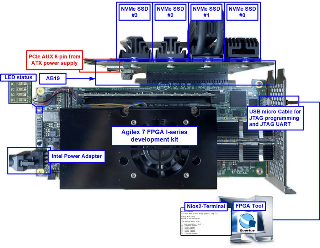
Figure 1‑3 NVMe-IP 4-ch RAID0 demo setup on Intel Agilex 7 FPGA I-series Development kit
2 Demo setup
2.1 Board setup
Follow these steps to set up the board for the demo.
1) Power off system.
2) Set SW3[3] to ON to select PCIe reference clock from PCIe connector.
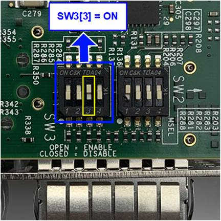
Figure 2‑1 Setting DIP Switch on FPGA board
3) Connect the AB19, NVMe SSD, and FPGA board by following these steps.
i) Check that the two mini jumpers at JP1 on AB19 are shorted between 1-3 and 2-4.
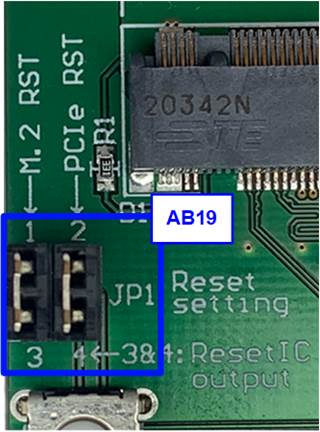
Figure 2‑2 Check jumpers on AB19
ii) Connect the NVMe SSDs to the AB19 board, as shown in Figure 2‑3.
a. For standard demo, connect the NVMe SSD to CN1: PCIe Lane3-0.
b. For 2-ch RAID0 demo, connect two NVMe SSDs to both CN1 and CN2.
c. For 4-ch RAID0 demo, connect four NVMe SSDs to all CNs (CN1-CN4).
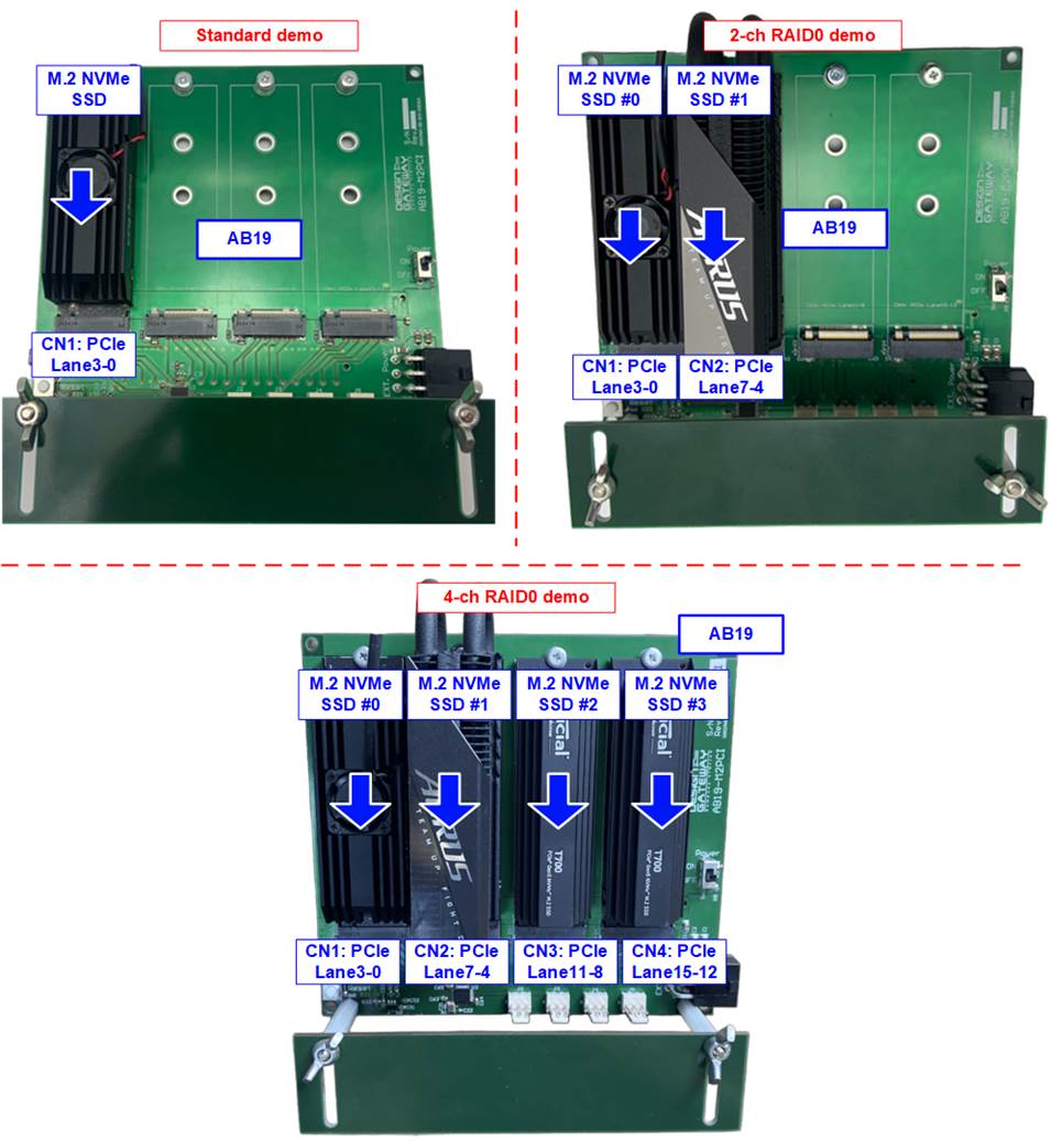
Figure 2‑3 Connect NVMe SSDs to AB19
iii) Connect the 6-Pin PCIe AUX from the ATX power supply to AB19-M2PCI as shown in Figure 2‑4.
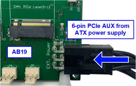
Figure 2‑4 Connect 6-Pin PCIe power supply to AB19
iv) Connect AB19 to the PCIe connector on the FPGA board.
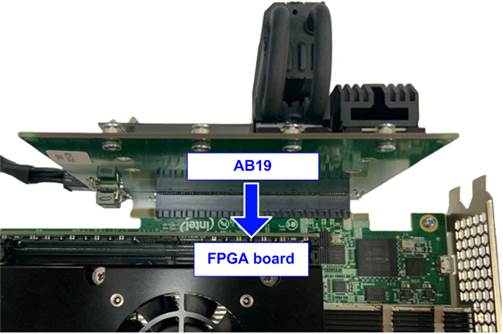
Figure 2‑5 Connect AB19 to FPGA board
v) Adjust the height of AB19 by sliding up-down the support board until AB19 is at the same vertical level as the PCIe connector on the FPGA board. Then, tighten the wing nut to fix the height.
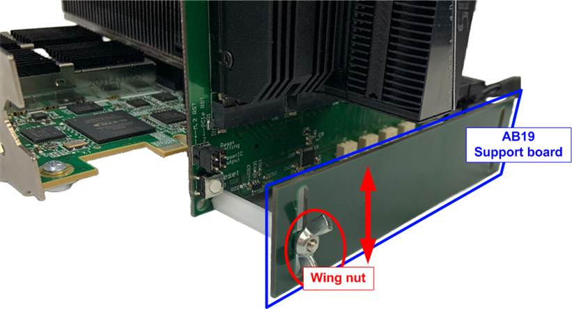
Figure 2‑6 Adjust the height of AB19 support board
4) Connect the micro USB cable from the FPGA board to the PC for JTAG programming and NiosII command shell.
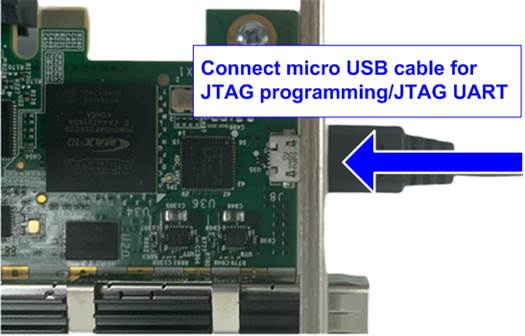
Figure 2‑7 micro USB cable connection
5) Connect the Intel power adapter to the FPGA board.
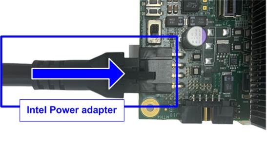
Figure 2‑8 Connect Intel power adapter to FPGA board
6) Turn on the power switch of the FPGA development board, AB19-M2PCI adapter board, and ATX power supply.
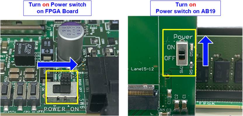
Figure 2‑9 Power on FPGA board and AB19 board
2.2 File Programming
Follow these steps to program the demo file to FPGA board.
1) Use Quartus Programmer to download the SOF file, as shown in Figure 2‑10.
a. For standard demo, use �NVMeIPG5Test_xxx.sof�.
b. For 2-ch RAID0 demo, use �NVMeIPG5RAID0x2Test_xxx.sof�.
c. For 4-ch RAID0 demo, use �NVMeIPG5RAID0x4Test_xxx.sof�.
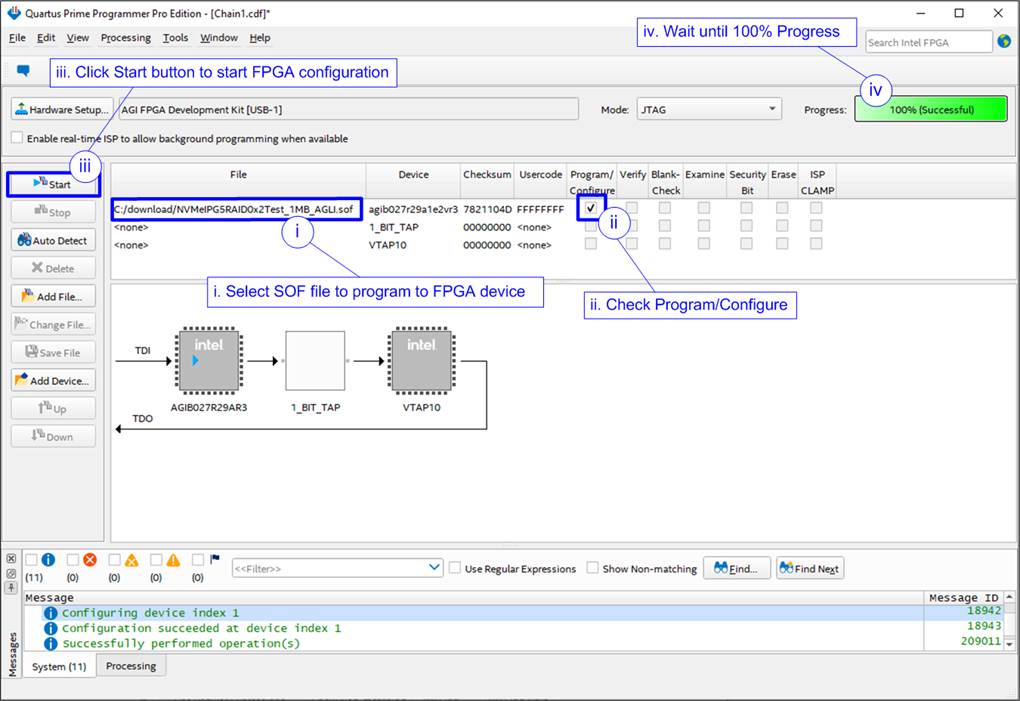
Figure 2‑10 Programmed by Quartus Prime Programmer
2) Launch NiosII Command Shell and input the command �nios2-terminal.exe -d 1�. This will display the boot message.
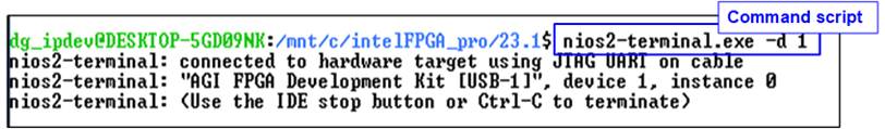
Figure 2‑11 The command for executing NiosII Terminal
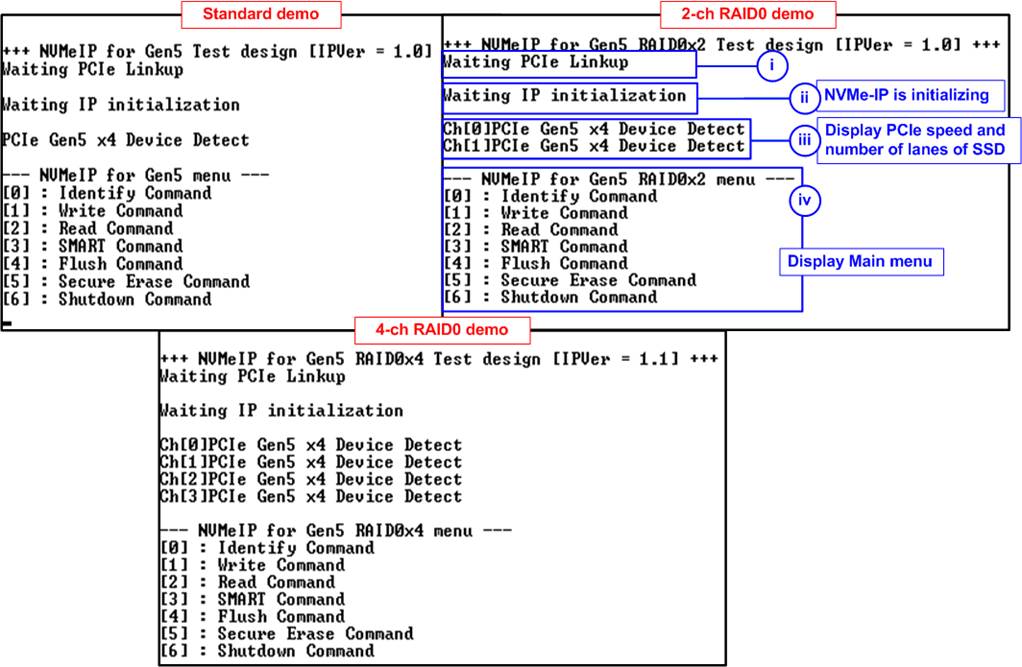
Figure 2‑12 NiosII Terminal after FPGA is completely configured
i) �Waiting PCIe Linkup� is displayed, indicating that the PCIe-IP linkup status is being monitored.
ii) Once the PCIe-IP link is established, �Waiting IP initialization� will be displayed, indicating that the NVMe-IP initialization is in progress.
iii) After the IP initialization is successful, the details of the PCIe connection for each SSD are presented, including the PCIe speed and the number of PCIe lanes. For this demo, it is expected to show PCIe Gen5 and 4 lanes.
iv) Finally, the main menu to execute the NVMe-IP commands is displayed. The user can select the test operation from this menu.
3) Check the LED status on the FPGA board. The LED description are as follows.
Table 2‑1 LED Definition
|
GPIO LED |
ON |
OFF |
|
0 |
Normal operation |
Clock is not locked |
|
1 |
System is busy |
Idle status |
|
2 |
IP Error detected |
Normal operation |
|
3 |
Data verification failed |
Normal operation |
4) After FPGA programming is complete, LED[0] and LED[1] will be ON when PCIe initialization is processing. LED[1] will turn OFF after the PCIe initialization process is complete, indicating that the system is ready to receive commands from user.
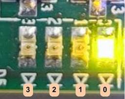
Figure 2‑13 LED Status for user output
3 Revision History
|
Revision |
Date |
Description |
|
1.2 |
3-Oct-23 |
Support 4-channel RAID0 demo |
|
1.1 |
28-Jun-23 |
Support 2-channel RAID0 demo |
|
1.0 |
3-May-23 |
Initial version release |