rmNVMe IP Core for Gen5 Data Sheet
PCIe Hard IP (R-Tile Avalon-ST Intel FPGA for PCIe)
Control interface (Single mode)
Control interface (Multiple mode)
Control interface (Parallel command)
Data stream interface (Parallel data)

Core Facts |
|
|
Provided with Core |
|
|
Documentation |
Reference Design Manual Demo Instruction Manual |
|
Design File Formats |
Encrypted File |
|
Instantiation Templates |
VHDL |
|
Reference Designs & Application Notes |
Quartus Project, See Reference Design Manual |
|
Additional Items |
Demo on Agilex7 I-Series development kit |
|
Support |
|
|
Support provided by Design Gateway Co., Ltd. |
|
Design Gateway Co.,Ltd
E-mail: ip-sales@design-gateway.com
URL: design-gateway.com
Features
· Directly access NVMe Gen5 SSD without CPU and external memory
· Two user interfaces (one-Write user and one-Read user) operating simultaneously
· Support seven commands.
· User#0 (Main user): Identify, Shutdown, SMART, Secure Erase, Flush, and Read commands
· User#1 (Sub user): Write command
· Support multiple Write and Read commands for 4Kbyte random access
· Configurable Command Depth of Write and Read commands independently: 32, 64, 128, 256
· Buffer size (depends on Command Depth): 128Kbyte (32 Commands) � 1Mbyte (256 Commands)
· Simple user interface by using Data stream interface
· Supported NVMe device
· Base Class Code:01h (mass storage), Sub Class Code:08h (Non-volatile), and Programming Interface:02h (NVMHCI)
· MPSMIN (Memory Page Size Minimum): 0 (4 Kbyte)
· MQES (Maximum Queue Entries Supported): At least (2 x Command Depth -1)
· LBA unit: 512 bytes
· User clock frequency: At least half of the PCIe clock frequency (250MHz for Gen5)
· PCIe Gen5 Hard IP: 256-bit interface using R-Tile Avalon-ST Intel FPGA for PCIe
· Available reference designs: Agilex7 I-Series development board with AB19-M2PCI adapter board
· Customized service for additional NVMe commands such as TRIM and Sanitize
Table 1: Example Implementation Statistics
|
Family |
Example Device |
U0/U1 Cmd Depth |
Fmax (MHz) |
Logic utilization (ALMs) |
Registers |
Pin |
Block Memory bit |
Design Tools |
|
Agilex7 I-Series |
AGIB027R29A1E2VR3 |
32 |
375 |
10,787 |
25,854 |
- |
2,410,240 |
Quartus 23.1 |
|
256 |
375 |
15,295 |
25,386 |
- |
17,113,344 |
Notes: Actual logic resource dependent on percentage of unrelated logic
Applications
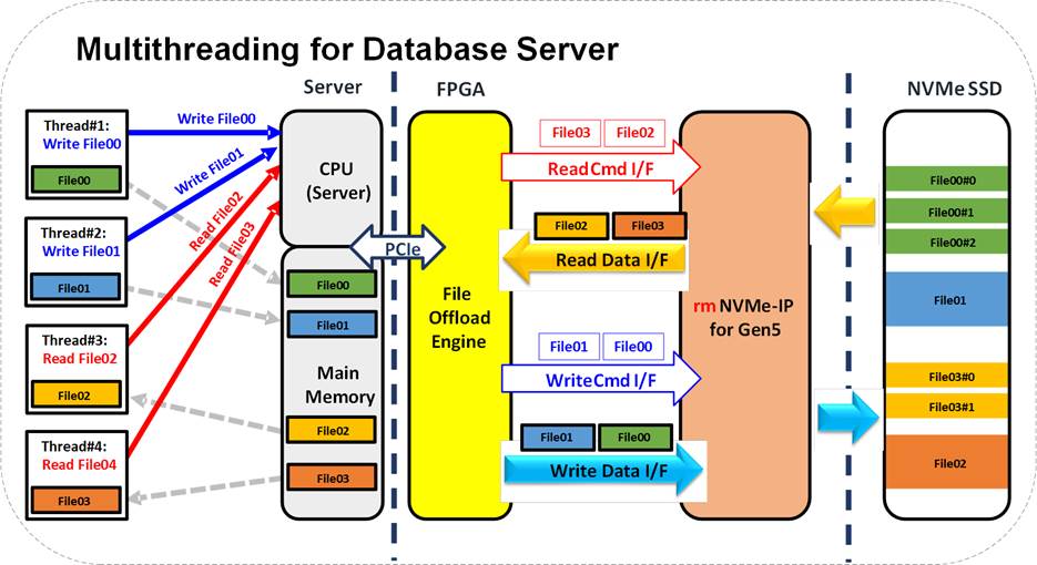
Figure 1: rmNVMe IP Application
The FPGA can be utilized as the offload engine for the database server to access storage, NVMe SSD. In large-scale systems, multiple threads frequently access the database, leading to a high volume of read and write requests being sent to the CPU. The write data, which is usually large in size, is stored in the main memory. The FPGA platform's PCIe engine provides an interface that allows the offload engine to receive command requests from the CPU and directly access the data in the main memory with high performance.
The File Offload Engine sends read and write requests to the rmNVMe IP via the Read Command Interface and Write Command Interface, respectively. All write data is transferred via the Write Data Interface and stored in the NVMe SSD. The read data from the NVMe SSD is returned to the File Offload Engine via the Read Data Interface and then directly returned to the thread through the main memory.
By utilizing this hardware system, the database can be accessed with high performance while requiring less CPU resources.
General Description
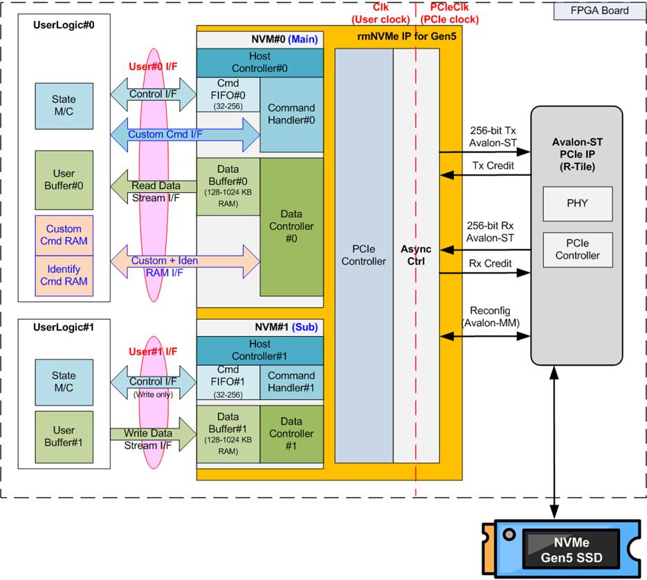
Figure 2: rmNVMe IP for Gen5 block diagram
The rmNVMe IP for Gen5 implements the NVMe host controller to access NVMe SSD with random access and two-user function. The physical interface of the NVMe SSD is PCIe, which is handled by PCIe Gen5 hard IP (R-Tile Avalon-ST Intel FGPA IP for PCIe).
The rmNVMe IP supports seven NVMe commands, i.e., Identify, Shutdown, Write, Read, SMART, Secure Erase, and Flush. These commands can be accessed through two user interfaces � User#0 I/F and User#1 I/F. The User#0 I/F represents the interface of NVM#0 module inside the rmNVMe IP, while the User#1 I/F represents the interface of NVM#1 module. NVM#0 (Main) supports various NVMe commands, including Identify, Shutdown, Read, SMART, Secure Erase, and Flush. While NVM#1 (Sub) supports only the Write command. Both User#0 I/F and User#1 I/F consist of two interface groups: the Control interface for transferring command and parameters, and the Data interface for transferring data when necessary.
The Control interface uses the FIFO interface to support multiple Write/Read command requests from the user with parameter assignments. The Data interface for Write/Read commands uses a Data stream interface, with a 512-bit data bus controlled by valid/ready/pause signal.
SMART, Secure Erase, and Flush command require a specific interface called the Custom command interface, which includes the Ctm I/F for Control path and the Ctm RAM I/F for Data path. Additionally, the Identify command has its own data interface, called the Iden RAM I/F. All of these specific interfaces are integrated only in the User#0 I/F.
Due to two user interfaces, while the Write command is operating in NVM#1, other commands such as Identify, Read, SMART, and Flush can be executed parallelly in NVM#0. However, there is one limitation regarding parallel operation: the Secure Erase and Shutdown command must be executed only after both NVM#0 and NVM#1 return to an idle state. Thus, the NVM#0 must not be requested to perform a Secure Erase or Shutdown command while NVM#1 is operating the Write command.
During the initialization process or when running certain commands, the rmNVMe IP may assert an error signal if abnormal conditions are detected. The IP includes an error status that provides additional details about the error condition. To recover from the error status, both the rmNVMe IP and SSD must be reset.
The rmNVMe IP incorporates asynchronous circuit to allow the user logic to operate in its individual clock domain, not PCIe clock. However, there is a limitation regarding the clock frequency of the user logic. When transmitting packets to the PCIe hard IP, data must be continuously sent between the start and end of the packet. To support this requirement, the user logic clock (Clk) frequency must be equal to or greater than half of the PCIe clock (PCIeClk) frequency. Therefore, the bandwidth on the user logic side is equal to or higher than the PCIe hard IP bandwidth. When operating at PCIe Gen5 speed, the user logic clock must be equal to or greater than 250MHz (assuming the PCIe clock frequency is set to 500MHz).
The reference designs on FPGA evaluation boards are available for evaluation purposes before making a purchase decision.
Functional Description

Figure 3: Operation Flow of rmNVMe IP
The operation flow of the rmNVMe IP can be divided into three phases: Initialization, Command operation, and No operation, as shown in Figure 3.
During the Initialization phase, NVM#0 is responsible to handle the process. In this phase, NVM#1 merely waits until the Initialization is completed. The Initialization step involves the following actions.
1) NVM#0 waits until PCIe is ready by monitoring the Linkup and Data Link active status from the PCIe IP core.
2) NVM#0 initiates the initialization process by initializing flow control, configuring the PCIe and NVMe registers. If any errors are detected during the setup process, NVM#0 switches the IP to the Inactive state.
Once the Initialization phase is completed, both user interfaces become idle and ready to receive commands from user. Commands can be requested through both User#0 I/F and User#1 I/F simultaneously. Additionally, multiple Read commands (to NVM#0) and multiple Write commands (to NVM#1) can be requested until the Cmd FIFOs are full. However, Secure Erase and Shutdown commands are exceptions because they require both NVMe#0 and NVM#1 to be in an Idle state before sending one of these command requests to User#0 I/F. While NVM#0 is performing Secure Erase, NVM#1 must not execute any Write commands. Once the shutdown is completed, both NVM#0 and NVM#1 enter to the Inactive state.
For a detailed description of each command�s operation flow in the Command operation phase of NVM#0 and NVM#1, please refer to Figure 4. The left side illustrates the operation of NVMe#0, which supports six commands, while right side demonstrates the operation of NVM#1, which supports the Write command.

Figure 4: Command Operation Flow of NVM#0 and NVM#1
NVMe#0
1) The first command from the user must be the Identify command (U0Cmd=000b) to update the LBASize (disk capacity).
2) The last command before powering down the system must be the Shutdown command (U0Cmd=001b). This command is recommended to ensure that the SSD is powered down in a proper sequence and all Write data is stored in the flash memory, not in the cache of the SSD. After the Shutdown command is executed, the rmNVMe IP and SSD enter the Inactive state and do not accept any commands until the IP is reset.
3) The data size of each Read command requested to NVM#0 (U0Cmd=011b) is fixed to 4K bytes. Multiple Read commands can be requested by the user until the Cmd FIFO#0 is full. Therefore, steps 3a) � 3b) of NVMe#0 can be repeated until all Read commands are completed.
a) The IP sends the Read command to the SSD.
b) The 4K-byte data of each Read command is transferred to the user in the same order as the Read command requests. After each 4K-byte data transfer is finished, one Read command is flushed from the Cmd FIFO. A new Read command can be requested if the Cmd FIFO is not full. If a new Read command exists in the Cmd FIFO, NVM#0 returns to step 3a) to process the next Read command. Once all Read data has been completely transferred, the Cmd FIFO is empty, and the IP returns to the Idle state.
4) For the SMART command (U0Cmd=100b and CtmSubmDW0-15=SMART), 512-byte data is returned after the operation is completed.
a) The IP sends the Get Log Page command to read SMART/Health information from the SSD.
b) A 512-byte data is returned from the SSD. The IP forwards the data through the Custom command RAM interface (CtmRamAddr=0x00 � 0x07).
5) For the Secure Erase command (U0Cmd =100b and CtmSubmDW0-15=Secure Erase), there is no data transferring during the operation.
a) The IP sends the Secure Erase command to the SSD.
b) The IP waits until the SSD returns the status to complete the operation.
6) For the Flush command (U0Cmd=110b), there is also no data transfer during the operation.
a) The IP sends Flush command to the SSD.
b) The IP waits until the SSD returns a status to indicate the completion of the operation.
NVMe#1
1) Similar to the Read command, the data size of each Write command is fixed at 4 Kbytes. The user sends a Write command request to NVM#1 by asserting U1CValid to 1b. While NVM#1 is executing a Write command, the user can request new Write commands until the Cmd FIFO#1 is full. NVM#1 repeats steps 1a) � 1c) until all Write commands are executed.
a) The IP waits until a 4K-byte Write data is sent by the user.
b) The IP sends the Write command to the SSD.
c) After the SSD returns a successful status for each Write command, one Write command is flushed from the Cmd FIFO. A new Write command can be requested if the Cmd FIFO is not full. If a new Write command exists in the Cmd FIFO, NVM#1 returns to step 1a). Once all Write commands have been completely executed, the Cmd FIFO is empty, and the IP returns to the Idle state.
2) After the Shutdown command is completed by NVM#0, the rmNVMe IP and SSD enter the Inactive state and do not accept the new command until the IP is reset.
To support multiple users and random access, the rmNVMe IP for Gen5 incorporates two protocols: the NVMe protocol for interfacing with the user and the PCIe protocol for interfacing with the PCIe hard IP. Therefore, the hardware within the rmNVMe IP is divided to two groups: NVMe and PCIe. Further details of each hardware module are described below.
NVMe
The rmNVMe IP supports seven commands: Identify, Write, Read, SMART, Secure Erase, Flush, and Shutdown. These commands are categorized into two groups: Single-mode commands and Multiple-mode commands. There are five Single-mode commands: Identify, SMART, Secure Erase, Flush, and Shutdown, which are exclusively supported in NVM#0 through the User#0 I/F. When the user sends a Single-mode command request to NVM#0 via the Cmd FIFO#0 interface, the command ready signal in the User#0 I/F is de-asserted, blocking the next command request from the user until the previous command is completed.
In contrast, there are two Multiple-mode commands: Write command and Read command. The maximum number of Read commands that can be requested to NVM#0 is configured by the User#0 Command Depth parameter, while the maximum number of Write commands that can be requested to NVM#1 is configured by the User#1 Command Depth parameter. The order of data transfer via the Data stream I/F is the same as the order of the Write/Read commands sent to Cmd FIFO (Control I/F). Additionally, the data transfer size of each Write/Read command is fixed at 4 Kbytes. Therefore, the Data Buffer size for NVM#0 and NVM#1 is equal to 4 Kbytes multiplied by the Command Depth parameter. For example, a 128-Kbyte buffer is used to support 32 Commands, and a 1-Mbyte buffer is used to support 256 Commands.
To implement the NVMe protocol, the NVM#0 and NVM#1 blocks are designed to have five submodules: Host Controller, Cmd FIFO, Command Handler, Data Buffer, and Data Controller. However, the submodule features and complexity between NVM#0 and NVM#1 are not exactly identical due to the differences in user command support. The details of each submodule are described as follows.
· Host Controller
The Host Controller is the core engine within the rmNVMe IP and is designed within each NVMe module. The module�s operation is divided into two phases. The first phase is the Initialization phase, which runs once after the system boots up to configure the NVMe register inside the SSD. This initialization process is only performed by Host Controller#0, as illustrated earlier in Figure 3. Once the Initialization phase is completed, the next phase is the Command operation phase.
During command execution, the Host controller manages the Command Handler. When a command involves data transfer such as Write, Read, SMART and Identify commands, the Host Controller also handles the Data Controller. It monitors the order of each packet type returned from the SSD and decodes the status value in the received packet to determine if the command has been executed successfully or if any errors have occurred. If errors are detected by the Host controller, the corresponding error status is returned to the user.
· Cmd FIFO
The Command FIFO (Cmd FIFO) allows for the configuration of the maximum number of Multiple-mode commands using the Command Depth parameters (U0CDep and U1CDep), as shown in Table 3. The Command Depth can be set to four values: 32, 64, 128, and 256, which determine the depth of Cmd FIFO#0 and Cmd FIFO#1 within the rmNVMe IP.
Cmd FIFO#0 is used to store the address of Read commands, while Cmd FIFO#1 is used for Write commands, enabling the operation of Multiple-mode commands. If the user intends to send a Single-mode command to NVMe#0, the user must wait until Cmd FIFO#0 is empty.
· Command Handler
The Command Handler is responsible for creating command packets and decoding the status packet returned from the SSD after the completion of each command. When the command is Identify, Shutdown, Write, or Read command, the parameters within the command packet are set by the internal registers. In case of SMART, Secure Erase, or Flush commands, the parameters are set via a 512-bit Custom command interface known as the Custom submission queue entry, which is defined by 16 DWORDs (where 1 DWORD = 32 bits).
The status of each command is returned through a Completion queue entry. The Command Handler provides three status outputs extracted from Completion queue entry for user monitoring: a 16-bit Admin completion status for Identify and Shutdown commands, a 32-bit IO completion status for Write and Read commands, and a 128-bit Custom completion status defined by 4 DWORDs for SMART, Secure Erase, and Flush commands.
· Data Buffer
rmNVMeIP utilizes two Data Buffers: Data Buffer#0 and Data Buffer#1. These Data Buffers are implemented by memory blocks. Data Buffer#0, integrated in NVM#0, stores the raw data of Read commands, while Data Buffer#1, integrated in NVM#1, stores the raw data of Write commands. The Data Buffers serve as storage for data transfer between the UserLogic and the SSD. The size of Data Buffer is determined by the Command Depth parameter because each Write/Read command requires a 4Kbyte buffer size, as indicated in Table 2.
Table 2: Data Buffer size of each Command Depth value
|
Command Depth |
Data Buffer size |
|
32 commands |
128 Kbyte |
|
64 commands |
256 Kbyte |
|
128 commands |
512 Kbyte |
|
256 commands |
1 Mbyte |
· Data Controller
The Data Controller module is responsible for data transfer in commands such as Identify, SMART, Write, and Read. It interfaces with the SSD through three data interfaces: the Data stream interface for Write and Read commands, the Custom command RAM interface for SMART command, and the Identify interface for Identify command.
For each Write/Read command, the Data Controller allocates a 4Kbyte size for data transfer. Additionally, it ensures that the order of the 4Kbyte data transferred between the user and the Data Buffer corresponds to the order of the Write/Read Commands from the user.
PCIe
The PCIe standard is an outstanding low-layer protocol specifically designed for high-speed applications. The NVMe standard operates over the PCIe protocol. During the initialization process, the NVMe layer is set up after completing the setup of the PCIe layer. Within rmNVMe IP, two modules are designed to support the PCIe protocol: PCIe Controller and AsyncCtrl. Further details about each module are described as follows.
· PCIe Controller
During the initialization process, PCIe Controller initializes flow control through Tx/Rx Credit port and sets up the PCIe environment of the SSD via the Reconfig port, which is the Avalon-MM interface. Subsequently, PCIe packets are created or decoded through the 256-bit Tx/Rx Avalon-Stream. The data flow in the Tx/Rx Avalon-Stream is controlled through Credit Control via the Tx/Rx Credit port. PCIe Controller is responsible for converting the command and data packets from the NVMe module into PCIe packets. Similarly, it decodes and converts received PCIe packets into NVMe packets for the NVMe module.
· AsyncCtrl
AsyncCtrl incorporates asynchronous registers and asynchronous buffers with asymmetric data width to facilitate clock domain crossing and support different data width. The data width on the user interface is twice that of the data width on the PCIe interface. This configuration enables the user clock frequency to be equal to or greater than half of the PCIe clock frequency, thereby achieving a balanced data bandwidth. Most logics within rmNVMe IP operates on the user clock domain, while the PCIe hard IP functions on the PCIe clock domain.
User Logic
The User Logic module can be designed using a small state machine to send commands and assign parameters for each command. With rmNVMe IP supporting multiple Write/Read commands, users can send commands to the Control interface (Cmd FIFO) and transfer data individually using the Stream interface (valid/ready signal). The output data of SMART and Identify commands can be mapped to a simple dual port RAM with byte enable. All data interfaces are 512-bit interfaces. The size of the data returned by the Identify command is 8 Kbytes, while the size of the data returned by the SMART command is 512 bytes.
PCIe Hard IP (R-Tile Avalon-ST Intel FPGA for PCIe)
To connect with the rmNVMe IP, five interfaces of the PCIe Hard IP (R-Tile Avalon-ST Intel FPGA for PCIe) are utilized: Avalon-ST RX Port (rx_st0/1_*) for receiving packets, Rx Credit Port (rx_st_*) for Rx flow control, Avalon-ST Tx Port (tx_st#_*) for transmitting packets, Tx Credit Port (tx_st_*) for Tx flow control, and Hard IP Reconfiguration (hip_reconfig_*) for PCIe configuration.
The PCIe hard IP implements the Transaction layer, Data Link layer, and Physical layer of the PCIe protocol. The maximum number of SSDs that can be connected to each FPGA device is determined by the number of PCIe hard IP blocks available. Each PCIe hard IP supports up to 16-lane PCIe Gen5 interface, which can be configured to four 4-lane PCIe Gen5 interfaces. Consequently, one PCIe Hard IP can connect with up to four rmNVMe IPs and four NVMe Gen5 SSDs.
For more details about the PCIe hard IP, please refer to the provided documentation.
https://www.intel.com/content/www/us/en/docs/programmable/683501/
Core I/O Signals
Descriptions of all signal I/O are provided in Table 3 - Table 6.
Table 3: Core Parameters
|
Name |
Value |
Description |
|
U0CDep |
5-8 |
The Command Queue Depth for NVM#0. Valid value is 5 - 8. Command Queue Depth = 2U0CDep. 5: 32 commands, 6: 64 commands, 7: 128 commands, 8: 256 commands. |
|
U1CDep |
5-8 |
The Command Queue Depth for NVM#1. Valid value is 5 - 8. Command Queue Depth = 2U1CDep. 5: 32 commands, 6: 64 commands, 7: 128 commands, 8: 256 commands. |
Table 4: User logic I/O Signals (Synchronous to Clk signal)
|
Signal |
Dir |
Description |
|
RstB |
In |
Synchronous reset signal. Active low. De-assert to 1b when the Clk signal is stable. |
|
Clk |
In |
User clock for running the rmNVMe IP. The frequency of Clk must be equal to or greater than half the frequency of PCIeClk signal, the clock output from the PCIe hard IP. If the PCIe hard IP operates at 500 MHz PCIe hard IP for Gen5 speed, Clk frequency must be 250 MHz or higher. |
|
U0Cmd[2:0] |
In |
User Command for User#0 I/F. Valid when U0CValid=1b. 000b: Identify, 001b: Shutdown, 011b: Read SSD, 100b: SMART/Secure Erase, 110b: Flush, Others: Reserved Note: User cannot switch to other commands when NVM#0 is busy. The user must wait until the current command is finished (U0Busy=0b). |
|
U0Addr[47:0] |
In |
Start address of User#0 I/F to read SSD in 512-byte units. Valid when U0CValid=1b. This value must be less than the SSD capacity (LBASize). Note: U0Addr[2:0] are ignored for 4-Kbyte alignment. |
|
U0CValid |
In |
Command valid. Assert to 1b to send a new Read command to NVM#0. For Single-mode commands (Identify, Shutdown, SMART, Secure Erase, and Flush), U0CReady is de-asserted to 0b after U0CValid is asserted. However, for Read commands, the user can assert U0CValid to send the next Read command until U0CReady is de-asserted to 0b. |
|
U0CReady |
Out |
Asserted to 1b to indicate that NVM#0 is ready to receive a command from User#0. |
|
U0Busy |
Out |
Busy status of User#0. Asserted to 1b when NVM#0 is operating a command from User#0 I/F. |
|
U0CCnt[8:0] |
Out |
Remaining count of Read commands stored in Cmd FIFO#0. Valid ranging from 0 to User#0 Command Depth. However, this signal is ignored for Single-mode commands. For example, if User#0 Command Depth is 32, U0CCnt can have values from 0 to 32. |
|
U0CId[7:0] |
Out |
Indicate the ID of Read Command in Cmd FIFO#0. Valid when U0CValid=1b. The value ranges from 0 to (User#0 Command Depth � 1). It is used to match with U0DId to refer the currently transferred command number in the Read Data stream interface of User#0 I/F. It is also used to match with the error ID of U0IOCompStatus[23:16]. This signal is ignored for Single-mode commands. For example, if User#0 Command Depth is 32, U0CId can have values from 0 to 31. |
|
U1Addr[47:0] |
In |
Start address of User#1 I/F to Write SSD in 512-byte units. Valid when U1CValid=1b. This value must be less than the SSD capacity (LBASize). Note: U1Addr[2:0] are ignored for 4-Kbyte alignment. |
|
U1CValid |
In |
Command valid. Asserted to 1b to send a new Write command to NVM#1. User can assert U1CValid to send the next Write command until U1CReady is de-asserted to 0b. |
|
U1CReady |
Out |
Asserted to 1b to indicate that NVM#1 is ready to receive Write command. |
|
U1Busy |
Out |
Busy status of User#1. Asserted to 1b when NVM#1 is operating a command from User#1 I/F. |
|
Signal |
Dir |
Description |
|
Control Interface of rmNVMe IP for Gen5 |
||
|
U1CCnt[8:0] |
Out |
Remaining count of Write commands stored in Cmd FIFO#1. Valid ranging from 0 to User#1 Command Depth. For example, when User#1 Command Depth is 32, U1CCnt can have values from 0 to 32. |
|
U1CId[7:0] |
Out |
Indicate the ID of Write Command in Cmd FIFO#1. Valid when U1CValid=1b. The value ranges from 0 to (User#1 Command Depth � 1). It is used to match with U1DId to refer the currently transferred command number in the Write Data stream interface of User#1 I/F. It is also used to match with the error ID of U1IOCompStatus[23:16]. For example, if User#1 Command Depth is 32, U1CId can have values from 0 to 31. |
|
LBASize[47:0] |
Out |
The total capacity of the SSD in 512-byte unit and always aligned to a 4 KB unit. This value is valid after Identify command is executed. Therefore, Identify command must be the first command issued by the user in order to update the LBASize value before running other commands. The default value after booting up is 0. |
|
U0-1Error |
Out |
Indicate an error. Asserted to 1b when U0-U1ErrorType is not equal to 0. The flag can be cleared by asserting RstB to 0b. |
|
U0ErrorType[31:0] |
Out |
Provide details about different error types. [0] � Error when the PCIe class code is incorrect. [1] � Error from the CAP (Controller capabilities) register, which may be caused by - MPSMIN (Memory Page Size Minimum) is not equal to 0. - NVM command set flag (bit 37 of CAP register) is not set to 1. - DSTRD (Doorbell Stride) is not equal to 0. - MQES (Maximum Queue Entries Supported) is less than (2 x User#0 Command Depth - 1) or (2 x User#1 Command Depth - 1). Further details of each register can be checked from NVMeCAPReg signal. [2] � Error when Admin completion entry is not received within timeout period. [3] � Error when status register in Admin completion entry is not 0 or the phase tag/command ID is invalid. Further details can be checked from U0AdmCompStatus signal. [4] � Error when IO completion entry of NVM#0 is not received within timeout period. [5] � Error when status register in IO completion entry of NVM#0 is not 0 or the phase tag is invalid. Further details can be checked from U0IOCompStatus signal. [6] � Error from unsupported LBA unit where the LBA unit is not equal to 512 bytes. [7] � Error when the number of queues supported by the SSD is less than 2. [8] � Error when receiving TLP packet with an incorrect size. [9] � Reserved Bit[15:10] are mapped to Uncorrectable Error Status Register. [10] � Mapped to Unsupported Request Error Status (bit[20]). [11] � Mapped to Completer Abort Status (bit[15]). [12] � Mapped to Unexpected Completion Status (bit[16]). [13] � Mapped to Completion Timeout Status (bit[14]). [14] � Mapped to Poisoned TLP Received Status (bit[12]). [15] � Mapped to ECRC Error Status (bit[19]). [23:16] � Reserved Bit[30:24] are also mapped to Uncorrectable Error Status Register. [24] � Mapped to Data Link Protocol Error Status (bit[4]). [25] � Mapped to Surprise Down Error Status (bit[5]). [26] � Mapped to Receiver Overflow Status (bit[17]). [27] � Mapped to Flow Control Protocol Error Status (bit[13]). |
|
Dir |
Description |
|
|
Control Interface of rmNVMe IP for Gen5 |
||
|
U0ErrorType[31:0] |
Out |
[28] � Mapped to Uncorrectable Internal Error Status (bit[22]). [29] � Mapped to Malformed TLP Status (bit[18]). [30] � Mapped to ACS Violation Status (bit[21]). [31] � Reserved. Note: Timeout period of bit[2]/[4] is set from TimeOutSet input. |
|
U1ErrorType[31:0] |
Out |
[3:0] � Reserved. [4] � Error when IO completion entry of NVM#1 is not received within timeout period. [5] � Error when status register in IO completion entry of NVM#1 is not 0 or the phase tag is invalid. Further details can be checked from U1IOCompStatus signal. [31:6] � Reserved. Note: Timeout period of bit[4] is set from TimeOutSet input. |
|
Data Stream Interface of rmNVMe IP for Gen5 |
||
|
U0DId[7:0] |
Out |
Indicate User#0 Command ID (U0CId) that is currently transferring data on the Read Data stream interface during Read commands. Valid when U0RdValid=1b. The value ranges from 0 to (User#0 Command Depth � 1). |
|
U0RdData[511:0] |
Out |
User#0 Read data returned from the SSD during Read commands. Valid when U0RdValid =1b. |
|
U0RdValid |
Out |
User#0 Read data valid that is asserted to 1b to transfer U0RdData. The user can pause the transmission by asserting U0RdPause to 1b. After that, U0RdValid is de-asserted to 0b within 4 clock cycles. |
|
U0RdPause |
In |
Assert to 1b to pause the transmission of U0RdData by de-asserting U0RdValid to 0b within 4 clock cycles. |
|
U1DId[7:0] |
Out |
Indicate User#1 Command ID (U1CId) that is currently transferring data on the Write Data stream interface during Write commands. Valid when U1WrValid=1b. The value ranges from 0 to (User#1 Command Depth � 1). |
|
U1WrData[511:0] |
In |
User#1 Write data to SSD during Write commands. Valid when U1WrValid=1b. |
|
U1WrValid |
In |
Assert to 1b to write data to NVM#1 for Write commands. Write data can be transferred before sending the Write command (U1CValid). |
|
U1WrReady |
Out |
Asserted to 1b when NVM#1 accepts the write data (U1WrData). |
|
U1WrCnt[14:0] |
Out |
Total data count of Write data stored in Data Buffer#1 in 512-bit unit. The value ranges from 0 to 64 times of User#1 Command Depth. |
|
rmNVMe IP for Gen5 Interface |
||
|
IPVesion[31:0] |
Out |
IP version number. |
|
U0TestPin[127:0], U1TestPin[15:0] |
Out |
Reserved to be IP Test point. |
|
TimeOutSet[31:0] |
In |
Timeout value for waiting for completion from the SSD. The time unit is equal to 1/(Clk frequency). When TimeOutSet is set to 0, the timeout feature is disabled. |
|
U0AdmCompStatus[15:0] |
Out |
Status output from Admin Completion Entry. [0] � Set to 1b when Phase tag or Command ID in Admin Completion Entry is invalid. [15:1] � Status field value of Admin Completion Entry. |
|
U0IOCompStatus[31:0] |
Out |
Status output from IO Completion Entry in NVM#0. [0] � Set to 1b when Phase tag in IO Completion Entry in NVM#0 is invalid. [15:1] � Status field value of IO Completion Entry in NVM#0. [23:16] � Command ID of IO Completion Entry in NVM#0, referred to U0CId. [31:24] � Reserved. |
|
Signal |
Dir |
Description |
|
rmNVMe IP for Gen5 Interface |
||
|
U1IOCompStatus[31:0] |
Out |
Status output from IO Completion Entry in NVM#1. [0] � Set to 1b when Phase tag in IO Completion Entry in NVM#1 is invalid. [15:1] � Status field value of IO Completion Entry in NVM#1. [23:16] � Command ID of IO Completion Entry in NVM#1, referred to U1CId. [31: 24] � Reserved. |
|
NVMeCAPReg[31:0] |
Out |
The parameter value of the NVMe capability register when U0ErrorType[1] is asserted to 1b. [15:0] � MQES (Maximum Queue Entries Supported). [19:16] � DSTRD (Doorbell Stride). [20] � NVM command set flag. [24:21] � MPSMIN (Memory Page Size Minimum). [31:25] � Undefined. |
|
Identify Interface (for User#0) |
||
|
IdenWrEn |
Out |
Asserted to 1b for sending data output from Identify command. |
|
IdenWrDWEn[15:0] |
Out |
Dword (32-bit) enable of IdenWrData. Valid when IdenWrEn=1b. Each bit corresponds to a Dword in IdenWrData. 1b: This Dword data is valid, 0b: This Dword data is not available. Bit[0], [1], �, [15] correspond to IdenWrData[31:0], [63:32], �, [511:480], respectively. |
|
IdenWrAddr[6:0] |
Out |
Index of IdenWrData in 512-bit unit. Valid when IdenWrEn=1b. Bit[6]=0b: 0x00-0x3F represents 4Kbyte Identify controller data. Bit[6]=1b: 0x40-0x7F represents 4Kbyte Identify namespace data |
|
IdenWrData[511:0] |
Out |
4Kbyte Identify controller data or Identify namespace data. Valid when IdenWrEn=1b. |
|
Custom interface (for User#0) |
||
|
CtmSubmDW0[31:0] � CtmSubmDW15[31:0] |
In |
16 Dwords of Submission queue entry for SMART/Secure Erase/Flush command. DW0: Command Dword0, DW1: Command Dword1, �, and DW15: Command Dword15. Valid when U0CValid=1b and U0Cmd=100b (SMART/Secure Erase) or 110b (Flush). |
|
CtmCompDW0[31:0] � CtmCompDW3[31:0] |
Out |
4 Dwords of Completion queue entry output from SMART/Secure Erase/Flush command. DW0: Completion Dword0, DW1: Completion Dword1, �, and DW3: Completion Dword3 |
|
CtmRamWrEn |
Out |
Asserted to 1b for sending data output from Custom command such as SMART command. |
|
CtmRamWrDWEn[15:0] |
Out |
Dword (32-bit) enable of CtmRamWrData. Valid when CtmRamWrEn=1b. Each bit corresponds to a Dword in CtmRamWrData. 1b: This Dword data is valid, 0b: This Dword data is not available. Bit[0], [1], �, [15] correspond to CtmRamWrData[31:0], [63:32], �, [511:480], respectively. |
|
CtmRamAddr[6:0] |
Out |
Index of CtmRamWrData when SMART data is received. Valid when CtmRamWrEn=1b. (Optional) Index to request data input from CtmRamRdData for customized Custom commands. |
|
CtmRamWrData[511:0] |
Out |
512-byte data output from SMART command. Valid when CtmRamWrEn=1b. |
|
CtmRamRdData[511:0] |
In |
(Optional) Data input for customized Custom commands. |
Table 5: Physical I/O Signals for PCIe Gen5 Hard IP (Synchronous to PCIeClk signal)
|
Signal |
Dir |
Description |
|
System and Hard IP status signals |
||
|
PCIeRstB |
In |
Synchronous reset signal. Active low. De-assert to 1b when PCIe hard IP is not in reset state. |
|
PCIeClk |
In |
Clock output from PCIe hard IP. It is recommended to configure it as 500 MHz for optimal performance. Lower clock speed reduces the PCIe interface bandwidth, which may result in lower performance. |
|
DlUp |
In |
Assert to 1b when Data Link layer of PCIe hard IP is ready for data transfer. |
|
PCIe Hard IP Rx Interface |
||
|
PCIeRxReady |
Out |
Asserted to 1b to indicate that the rmNVMe IP is ready to accept data. This signal is always set to 1b. The Rx flow control is handled through the Rx Credit Interface. |
|
PCIeRxHdValidL |
In |
Assert to 1b to indicate that PCIeRxHdL is valid. |
|
PCIeRxDValidL |
In |
Assert to 1b to indicate that PCIeRxDataL is valid. |
|
PCIeRxSOPL |
In |
Assert to 1b to indicate that this is the first cycle of the TLP starting in the lower segment. Valid when PCIeRxHdValidL or PCIeRxDValidL is asserted to 1b. |
|
PCIeRxEOPL |
In |
Assert to 1b to indicate that this is the last cycle of the TLP ending in the lower segment. Valid when PCIeRxHdValidL or PCIeRxDValidL is asserted to 1b. |
|
PCIeRxHdL[127:0] |
In |
Received header data in the lower segment. Valid when PCIeRxHdValidL and PCIeRxSOPL are asserted to 1b. |
|
PCIeRxDataL[127:0] |
In |
Received data in the lower segment. Valid when PCIeRxDValidL is asserted to 1b. |
|
PCIeRxEmptyL[1:0] |
In |
Specific the number of empty Dwords of PCIeRxDataL when the TLP ends in the lower segment. Valid when PCIeRxDValidL and PCIeRxEOPL are asserted to 1b. |
|
The signals in the upper segment have the same description as the signals in the lower segment. The upper segment signals include PCIeRxHdValidH, PCIeRxDValidH, PCIeRxSOPH, PCIeRxEOPH, PCIeRxHdH[127:0], PCIeRxDataH[127:0], and PCIeRxEmptyH[1:0]. |
||
|
PCIe Hard IP Tx Interface |
||
|
PCIeTxReady |
In |
Assert to 1b to indicate that the PCIe hard IP is ready to receive data. If it is de-asserted to 0b, PCIeTxHdValidL/H and PCIeTxDValidL/H must be de-asserted to 0b within 16 clock cycles. When PCIeTxReady is re-asserted to 1b, PCIeTxDValidL/H must be re-asserted to 1b within 1 clock cycle to continue packet transmission. |
|
PCIeTxHdValidL |
Out |
Asserted to 1b to indicate that PCIeTxHdL is valid. When PCIeTxReady is de-asserted, this signal must be de-asserted within 16 clock cycles. |
|
PCIeTxDValidL |
Out |
Asserted to 1b to indicate that PCIeTxDataL is valid. When PCIeTxReady is de-asserted, this signal must be de-asserted within 16 clock cycles. When PCIeTxReady is re-asserted, this signal must be re-asserted within 1 clock cycle to continue packet transmission. |
|
PCIeTxSOPL |
Out |
Asserted to 1b to indicate the first cycle of a TLP in the lower segment. Valid when PCIeTxHdValidL or PCIeTxDValidL is asserted to 1b. |
|
PCIeTxEOPL |
Out |
Assert to 1b to indicate the last cycle of a TLP ending in the lower segment. Valid when PCIeTxHdValidL or PCIeTxDValidL is asserted to 1b. |
|
PCIeTxHdL[127:0] |
Out |
Transmitted header data in the lower segment. Valid when PCIeTxHdValidL and PCIeTxSOPL are asserted to 1b. |
|
PCIeTxDataL[127:0] |
Out |
Transmitted data in the lower segment. Valid when PCIeTxDValidL is asserted to 1b. |
|
The signals in the upper segment have the same description as the signals in the lower segment. The upper segment signals include PCIeTxHdValidH, PCIeTxDValidH, PCIeTxSOPH, PCIeTxEOPH, PCIeTxHdH[127:0], and PCIeTxDataH[127:0]. |
||
|
Signal |
Dir |
Description |
|
PCIe Hard IP Rx Credit Interface |
||
|
RxHCdInit[2:0] |
Out |
Asserted to 1b to request and indicate initialization phase of each Rx header credit type. De-assertion from 1b to 0b indicates the completion of the header credit initialization. [0] � Posted Header [1] � Non-Posted Header [2] � Completion Header |
|
RxHCdAck[2:0] |
In |
The response of RxHCdInit. Assert to 1b to indicate that PCIe hard IP is ready for initialization of the Rx header credit. Bit[0], [1], and [2] correspond to RxHCdInit [0], [1], and [2], respectively. |
|
RxHCdCntValid[2:0] |
Out |
Valid of RxHCdCnt to release credit. Bit[0], [1], and [2] correspond to RxHCdCnt[1:0], [3:2], and [5:4], respectively. |
|
RxHCdCnt[5:0] |
Out |
Number of released header credit in the Rx side. [1:0] � Posted Header, valid when RxHCdCntValid[0] is asserted to 1b. [3:2] � Non-Posted Header, valid when RxHCdCntValid[1] is asserted to 1b. [5:4] � Completion Header, valid when RxHCdCntValid[2] is asserted to 1b. |
|
RxDCdInit[2:0] |
Out |
Asserted to 1b to request and indicate initialization phase of each Rx data credit type. De-assertion from 1b to 0b indicates the completion of the data credit initialization. [0] � Posted Data [1] � Non-Posted Data [2] � Completion Data |
|
RxDCdAck[2:0] |
In |
The response of RxDCdInit. Assert to 1b to indicate that the PCIe hard IP is ready for initialization of the Rx data credit. Bit[0], [1], and [2] correspond to RxDCdInit [0], [1], and [2], respectively. |
|
RxDCdCntValid[2:0] |
Out |
Valid of RxDCdCnt to release credit. Bit[0], [1], and [2] correspond to RxDCdCnt[3:0], [7:4], and [11:8], respectively. |
|
RxDCdCnt[11:0] |
Out |
Number of released data credit in the Rx side. [3:0] � Posted Data, valid when RxDCdCntValid[0] is asserted to 1b. [7:4] � Non-Posted Data, valid when RxDCdCntValid[1] is asserted to 1b. [11:8] � Completion Data, valid when RxDCdCntValid[2] is asserted to 1b. |
|
PCIe Hard IP Tx Credit Interface |
||
|
TxHCdInit[2:0] |
In |
Assert to 1b to request and indicate initialization phase of each Tx header credit type. De-assertion from 1b to 0b indicates the completion of the header credit initialization. [0] � Posted Header [1] � Non-Posted Header [2] � Completion Header |
|
TxHCdAck[2:0] |
Out |
The response of TxHCdInit. Asserted to 1b to indicate that rmNVMe IP is ready for initialization of the Tx header credit. Bit[0], [1], and [2] correspond to TxHCdInit [0], [1], and [2], respectively. |
|
TxHCdCntValid[2:0] |
In |
Valid of TxHCdCnt to release credit. Bit[0], [1], and [2] correspond to TxHCdCnt[1:0], [3:2], and [5:4], respectively. |
|
TxHCdCnt[5:0] |
In |
Number of released header credit in the Tx side. [1:0] � Posted Header, valid when TxHCdCntValid[0] is asserted to 1b. [3:2] � Non-Posted Header, valid when TxHCdCntValid[1] is asserted to 1b. [5:4] � Completion Header, valid when TxHCdCntValid[2] is asserted to 1b. |
|
Signal |
Dir |
Description |
|
PCIe Hard IP Tx Credit Interface |
||
|
TxDCdInit[2:0] |
In |
Assert to 1b to request and indicate initialization phase of each Tx data credit type. De-assertion from 1b to 0b indicates the completion of the data credit initialization. [0] � Posted Data [1] � Non-Posted Data [2] � Completion Data |
|
TxDCdAck[2:0] |
Out |
The response of TxDCdInit. Asserted to 1b to indicate that rmNVMe IP is ready for initialization of the Tx data credit. Bit[0], [1], and [2] correspond to TxDCdInit [0], [1], and [2], respectively. |
|
TxDCdCntValid[2:0] |
In |
Valid of TxDCdCnt to release credit. Bit[0], [1], and [2] correspond to TxDCdCnt[3:0], [7:4], and [11:8], respectively. |
|
TxDCdCnt[11:0] |
In |
Number of released data credit in the Tx side. [3:0] � Posted Data, valid when TxDCdCntValid[0] is asserted to 1b. [7:4] � Non-Posted Data, valid when TxDCdCntValid[1] is asserted to 1b. [11:8] � Completion Data, valid when TxDCdCntValid[2] is asserted to 1b. |
Table 6: PCIe Hard IP Reconfiguration and Link Status Signals (Synchronous to CfgClk signal)
|
Signal |
Dir |
Description |
|
System and Link status signal |
||
|
CfgRstB |
In |
Synchronous reset signal. Active low. De-assert this signal to 1b when the PCIe hard IP is not in reset state. |
|
CfgClk |
In |
Clock output from the PCIe hard IP. This clock value can be configured via divide-by-2 or divide-by-4 from PCIeClk. |
|
PCIeLinkup |
In |
Asserted to 1b when LTSSM state of the PCIe hard IP is in L0 State. |
|
LinkSpeed[2:0] |
Out |
Negotiated PCIe link speed that is read out from the PCIe Hard IP Reconfiguration Space. 000b: Undefined, 001b: Gen1, 010b: Gen2, 011b: Gen3, 100b: Gen4, 101b: Gen5, 110b/111b: Reserved. This register is valid after the rmNVMe IP has finished initialization (U0/U1Busy=0b). |
|
LinkWidth[1:0] |
Out |
Negotiated PCIe link width that is read out from the PCIe Hard IP Reconfiguration Space. 00b: Undefined, 01b: x1 lane, 10b: x2 lane, 11b: x4 lane. This register is valid after the rmNVMe IP has finished initialization (U0/U1Busy=0b). |
|
Reconfiguration Interface |
||
|
CfgAddr[31:0] |
Out |
Reconfiguration address for writing or reading. |
|
CfgWr |
Out |
Asserted to 1b to send a Write request. |
|
CfgWrData[7:0] |
Out |
Write data. Valid when CfgWrite=1b. |
|
CfgRd |
Out |
Asserted to 1b to send a Read request |
|
CfgRdData[7:0] |
In |
Read data. Valid when CfgRdValid=1b. |
|
CfgRdValid |
In |
Assert to 1b when CfgRdData is valid. |
|
CfgWaitRequest |
In |
Assert to 1b to indicate that the PCIe Hard IP is not ready to respond to a request. |
Timing Diagram
Initialization

Figure 5: Timing diagram during initialization process
The initialization process of the rmNVMe IP follows the steps below as shown in timing diagram.
1) Wait until Clk is stable and then de-assert RstB to 1b.
2) After completing the PCIe reset sequence, the PCIe hard IP de-asserts PCIeRstB and CfgRstB to 1b, indicating that it is ready to transfer data with the application layer.
3) The PCIe hard IP initiates the PCIe initialization by following steps.
a. The PCIeLinkup requires to run on CfgClk. However, it is decoded from the LTSSM signal, which is generated on PCIeClk. As a result, an asynchronous register must be used to set PCIeLinkup to 1b after the LTSSM state enters L0 state.
b. The PCIe hard IP then asserts DlUp to 1b when the Data Link layer becomes active.
After that, the rmNVMe IP initiates its own initialization process.
4) Upon completion of the initialization process, the IP de-asserts U0Busy and U1Busy to 0b. Also, U0CReady and U1CReady are asserted to 1b, indicating readiness to receive new commands from the user.
5) Afterward, the user can read the PCIe link speed and link width from the rmNVMe IP. However, these registers are synchronous with CfgClk and must be converted to the user logic clock domain using asynchronous registers.
Once the above sequences are finished, rmNVMe IP is ready to receive commands from the user.
Control interface (Single mode)
The rmNVMe IP supports two command types: Single mode and Multiple mode. In the Single-mode command, only the User#0 I/F is utilized, while the User#1 I/F supports only Write command (the Multiple-mode command). To initiate a Single-mode command, NVM#0 must be in Idle state (U0Busy=0b and U0CReady=1b). During the execution of a Single-mode command, User#0 I/F cannot receive new command requests until the ongoing Single-mode command operation is completed.

Figure 6: Control interface of dgIF typeS timing diagram
Figure 6 shows timing diagram when executing Single-mode commands (Identify, Shutdown, SMART, Secure Erase, and Flush) in NVM#0.
1) Before sending a new command to NVM#0, the user must check that U0Busy=0b and U0CReady=1b to ensure that NVM#0 of the rmNVMe IP is in an Idle state. Subsequently, U0CValid is asserted to 1b for one clock cycle along with a valid U0Cmd and the required command-specific parameters.
Note: SMART, Secure Erase, and Flush commands require the parameters CtmSubmDW0-DW15.
Identify and Shutdown commands do not require any parameters.
2) Upon receiving the new command request, NVM#0 asserts U0Busy to 1b and initiates the command operation. Simultaneously, U0CReady is de-asserted to 0b to block further new command requests.
3) After completing the command operation, U0Busy is de-asserted to 0b, and U0CReady is re-asserted to 1b. However, in the case of a Shutdown command, U0Busy remains de-asserted to 0b, while U0CReady is also de-asserted to 0b when Shutdown is completely executed. In this scenario, no further commands can be requested from the user.
Note: In Single-mode commands, U0Busy is de-asserted to 0b after U0CReady is asserted for 1 clock cycle, indicating the completion of the command operation. The user can then send a new command request after U0Busy is de-asserted.
Control interface (Multiple mode)
The Control interface of the rmNVMe IP supports two Multiple-mode commands: Read command by User#0 I/F and Write command by User#1 I/F. In comparison to the Single-mode command, the user can send multiple command requests by asserting U0CValid/U1CVaild to 1b if U0CReady/U1CReady is asserted to 1b. There is no need to wait for U0Busy/U1Busy to be de-asserted to 0b, unlike in the Single-mode command. The maximum number of Read commands and Write commands can be configured individually using U0CDep and U1CDep. The details of the Control interface for sending commands are as follows.

Figure 7: Multiple-mode command timing diagram by User#0 I/F
Since the timing diagram for sending a Read command request on the User#0 I/F and a Write command request on the User#1 I/F are similar, Figure 7 illustrates the timing diagram for the User#0 I/F when NVM#0 of the rmNVMe IP executes a Read command (Multiple-mode command) with assigning U0CDep = 5 (maximum 32 commands).
1) If the previous command is not a Read command, the user must ensure that NVM#0 is idle (U0Busy=0b) and Cmd FIFO#0 is ready (U0CReady=1b). Next, the user sends a Read command (U0Cmd=011b) to NVM#0 by asserting U0CValid to 1b for one clock cycle, along with the valid U0Addr.
2) NVM#0 initiates the command operation by asserting U0Busy to 1b. Meanwhile, U0CCnt and U0CId are incremented to indicate the number of commands in Cmd FIFO#0 and the next command ID, respectively.
3) As long as Cmd FIFO#0 is not full (U0CCnt is less than 32 or U0CReady=1b), the user can request Read command with new address value. U0Cmd must always be set to Read command when asserting U0CValid to 1b while the NVM#0 is busy (U0Busy=1b). Incorrect operation will occur if the user assigns a different value to U0Cmd while U0Busy=1b.
4) Once Cmd FIFO#0 is full (U0CCnt = User#0 Command Depth), U0CReady is de-asserted to 0b. NVM#0 no longer accepts command requests from the user. All inputs for the new command request must retain the same value until U0CReady is re-asserted.
5) After some Read commands are completed and Cmd FIFO#0 is not full (U0CCnt < User#0 Command Depth), U0CReady is re-asserted. If a new command is requested, NVM#0 will accept it.
6) When NVM#0 of the rmNVMe IP finishes processing all the command requests, U0Busy is de-asserted to 0b, and NVM#0 returns to the Idle status. At this point, NVM#0 is ready to receive a new command, which can be a Single-mode command.
Note: The User#1 I/F only supports the Write command, so there is no U1Cmd input signal for requesting the Write command to NVM#1.
Control interface (Parallel command)

Figure 8: Control interface when running command parallelly
Both User#0 I/F and User#1 I/F have specific control signals to operate user command simultaneously. Figure 8 illustrates the Control interfaces of the two user interfaces when NVM#0 and NVM#1 execute commands in parallel. This allows commands such as Identify, SMART, Flush, and Read in NVM#0 to be executed concurrently with the Write command in NVM#1. However, the Shutdown and Secure Erase command are an exception to this parallel mode and cannot be executed concurrently with other commands.
Read Data stream interface
The Read Data stream interface of rmNVMe IP is available in User#0 I/F and is responsible for transferring data during Read commands. This interface consists of two control signals: valid and pause.

Figure 9: Read Data stream interface
1) Once NVM#0 receives the 4 KB data from the SSD for the current command ID, it sends the 4 KB data to the user by asserting U0RdValid to 1b along with valid U0RdData. To transfer the entire 4 KB data, U0RdValid remains asserted to 1b for 64 consecutive clock cycles, assuming U0RdPause is consistently de-asserted to 0b.
2) After completing the transfer of each 4 KB data block, U0DId is incremented to indicate the command ID of the next 4 KB data block to be transferred.
Note: When the Command Depth is set to 32, U0DId ranges from 0 to 31.
3) The transfer of the next 4 KB data block occurs after the SSD returns the 4KB data, following the same process as in step 1).
4) If the user is not ready to receive read data, they can assert U0RdPause to 1b. In response, NVM#0 pauses the data transfer by de-asserting U0RdValid to 0b within 4 clock cycles.
5) When the user is ready to resume receiving read data, the user de-asserts U0RdPause to 0b. NVM#0 then re-asserts U0RdValid to 1b within 4 clock cycles to resume the data transfer.
Write Data stream interface
The Write Data stream interface in the User#1 I/F of the rmNVMe IP is responsible for transferring data during Write commands. This interface operates independently from the Control interface and allows the user to prepare Write data in Data Buffer#1 before or after sending the Write command request. Figure 10 illustrates timing diagram of Write command with a User#1 Command Depth configured to 5 (maximum 32 commands).

Figure 10: Write Data stream interface
1) Before initiating the data transfer, the user verifies that NVM#1 is ready to receive data by monitoring U1WrReady=1b or ensuring U1WrCnt < 64xUser#1 Command Depth (2048). Once confirmed, the user asserts U1WrValid along with valid U1WrData to transfer 512-bit data. Two status signals, U1WrReady and U1WrCnt, serve as flow control signals for the Write command. U1WrCnt is recommended for burst data transfer, while U1WrReady is suitable for non-burst data transfer.
2) After completing the transfer of a 4K-byte data block (the data size of each Write command), U1DId is incremented to indicate the command ID of the next 4K-byte data to be transferred through the Write Data stream interface (U1WrData).
3) If the user is not ready to send data, they can de-assert U1WrValid to 0b, effectively pausing the data transfer.
4) When the Data Buffer#1 becomes full (U1WrCnt reaches 64xUser#1Command Depth or 2048), U1WrReady is de-asserted to 0b. Consequently, NVM#1 cannot accept new data from the user. Both U1WrData and U1WrValid must maintain the same value until U1WrReady is re-asserted to 1b.
5) Once the previous Write command is complete, creating a 4 KB free space in the Data Buffer, U1WrCnt is reduced by 4 KB, and U1WrReady is re-asserted to 1b. This allows NVM#1 to accept data for the next command.
Data stream interface (Parallel data)

Figure 11: Data stream interface when transferring Read and Write parallelly
The Data stream interfaces for Read and Write operations in NVM#0 and NVM#1, respectively, operate independently. This parallel data transfer capability allows for concurrent Read and Write operations, as shown in Figure 11. The Read Data stream interface enables the return of Read data from NVM#0 while the user simultaneously sends Write data to NVM#1.
IdenCtrl/IdenName
To ensure proper operation of the system, it is recommended to send the Identify command to the IP as the first command after the system boots up. This command updates SSD total capacity (LBASize) which is necessary for Write and Read commands to operate correctly. The address (U0Addr/U1Addr) must not exceed the total capacity (LBASize) of the SSD.

Figure 12: Identify command timing diagram
When executing the Identify command, the following steps are operated.
1) The user sends a request for the Identify command to NVM#0 of the IP by setting U0Cmd=000b and asserting U0CValid=1b.
2) The IP asserts U0Busy to 1b upon receiving the command request. Simultaneously, U0CReady is de-asserted to 0b, indicating that new command requests from the user will be ignored until the current command is completed.
3) The IP returns a 4096-byte Identify controller data to the user with IdenWrAddr equal to 0-63 and asserts IdenWrEn. IdenWrData and IdenWrDWEn are valid at the same clock as IdenWrEn=1b.
4) The IP returns 4096-byte Identify namespace data to the user with IdenWrAddr equal to 64-127. IdenWrAddr[6] can be used to determine the data type as Identify controller data or Identify namespace data.
5) Upon completion the Identify command operation, the IP de-asserts U0Busy to 0b, along with a valid LBASize. Also, U0CReady is re-asserted to 1b, enabling the reception of new commands.
Note: U0Busy is de-asserted to 0b after U0CReady is asserted for 1 clock cycle, signaling the completion of the operation.

Figure 13: IdenWrDWEn timing diagram
The signal IdenWrDWEn is 16-bit signal used to validate a 32-bit data signal. Some SSDs return the 4-Kbyte Identify controller data and Identify namespace data one word (32-bit) at a time instead of continuously. To forward 32-bit data, one bit of IdenWrDWEn is asserted to 1b in the write cycle, as illustrated in Figure 13. Each bit of IdenWrDWEn (IdenWrDWEn[0], [1], �, [15]) corresponds to each 32-bit data of IdenWrData (IdenWrData[31:0], [63:32], �, [511:480]).
Shutdown
The Shutdown command is a command that should be sent as the last command before the system is powered down. The SSD ensures that the data from its internal cache is written to the flash memory before the shutdown process finishes. After the shutdown operation is completed, the rmNVMe IP and the SSD become inactive status. If the SSD is powered down without executing the Shutdown command, the total count of unsafe shutdowns is increased, as returned data from the SMART command.

Figure 14: Shutdown command timing diagram
The process for executing the Shutdown command is described below.
1) Before requesting the Shutdown command, both NVM#0 and NVM#1 must be in the Idle state, indicated by U0Busy=0b, U1Busy=0b, and U0CReady=1b. To send Shutdown command, the user asserts U0CValid to 1b and sets U0Cmd=001b.
2) Upon receiving the Shutdown command, the IP asserts U0Busy to 1b, indicating that it is processing the command. Additionally, both U0CReady and U1CReady are de-asserted to 0b, preventing any new command requests.
3) After the completion of the Shutdown command operation, U0Busy is de-asserted to 0b, indicating that the IP is no longer busy. However, U0CReady and U1CReady remain at 0b because the IP does not accept any commands after the Shutdown command.
SMART
The SMART command is the command to check the health of the SSD. When this command is sent, the SSD returns 512-byte health information. The SMART command parameters are loaded from the CtmSubmDW0-DW15 signals on the Custom command interface. The user must set the 16-Dword data which is a constant value before asserting U0CValid. Once the SMART data is returned, it can be accessed via the CtmRAM port, as shown in Figure 15.

Figure 15: SMART command timing diagram
To execute the SMART command, follow these steps.
1) Ensure that NVM#0 of the IP is ready to receive command by checking that U0Busy=0b and U0CReady=1b. Then, asserts U0CValid with U0Cmd=100b and set the following values to CtmSubmDW0-DW15 for the SMART command.
CtmSubmDW0 = 0x0000_0002
CtmSubmDW1 = 0xFFFF_FFFF
CtmSubmDW2 � CtmSubmDW5 = 0x0000_0000
CtmSubmDW6 = 0x0802_2000
CtmSubmDW7 � CtmSubmDW9 = 0x0000_0000
CtmSubmDW10 = 0x007F_0002
CtmSubmDW11 � CtmSubmDW15 = 0x0000_0000
2) NVM#0 acknowledges the SMART command by asserting U0Busy to 1b and de-asserting U0CReady to 0b.
3) Receive the 512-byte SMART data on the CtmRamWrData signal. The valid SMART data is indicated by asserting CtmRamWrEn to 1b. The CtmRamAddr corresponds to the data index of the 512-byte data (0-7). When CtmRamAddr=0, bytes 0-63 of the SMART data are valid on CtmRamWrData. The CtmRamWrDWEn is used as Dword enable for each 32-bit CtmRamWrData. If CtmRamWrDWEn=FFFFh, all 512 bits of CtmRamWrData are valid.
4) Once the SMART command operation is completed, de-assert U0Busy to 0b and assert U0CReady to 1b to indicate readiness for the next command.
Note: U0Busy is de-asserted to 0b after U0CReady is asserted for 1 clock cycle to indicate the completion of the operation.

Figure 16: CtmRamWrDWEn timing diagram
Similar to Identify command, some SSDs may not return the 512-byte data continuously, but instead return one Dword (32-bit) at a time. In this case, each write cycle should have one bit of CtmRamWrDWEn asserted to 1b, serving as the valid signal for the corresponding 32-bit CtmRamWrData. CtmRamWrDWEn[0], [1], �, [15] correspond to CtmRamWrData[31:0], [63:32], �, [511:480], respectively.
Secure Erase
Secure Erase is a command that erases all user data in the SSD. After the Secure Erase command is executed, the contents of the user data are indeterminate.

Figure 17: Secure Erase command timing diagram
Below are the details of how to run the Secure Erase command.
1) Ensure that both NVM#0 and NVM#1 are in the Idle state, indicated by U0Busy=0b, U1Busy=0b, and U0CReady=1b. To send the Secure Erase command request, the user asserts U0CValid with U0Cmd=100b and assign the following values to CtmSubmDW0-DW15.
CtmSubmDW0 = 0x0000_0080
CtmSubmDW1 = 0x0000_0001
CtmSubmDW2 � CtmSubmDW9 = 0x0000_0000
CtmSubmDW10 = 0x0000_0200
CtmSubmDW11 � CtmSubmDW15 = 0x0000_0000
2) NVM#0 of the IP accepts the Secure Erase command by asserting U0Busy to 1b and de-asserting U0CReady to 0b.
3) Once the Secure Erase command operation is completed, U0Busy is de-asserted to 0b and U0CReady is asserted to 1b to be ready for the next command.
Note: U0Busy is de-asserted to 0b after U0CReady is asserted for 1 clock cycle to indicate the completion of the operation.
Note: Some SSDs may encounter a decrease in performance after long data transfer. In such cases, the Secure Erase command can assist in restoring their performance.
Flush
The SSDs typically enhance write performance by caching write data before writing it to the flash memory. However, unexpected power loss can result data loss as cached data may not be stored in flash memory. To avoid data loss, the Flush command can be used to force the SSD controller to write cached data to the flash memory.
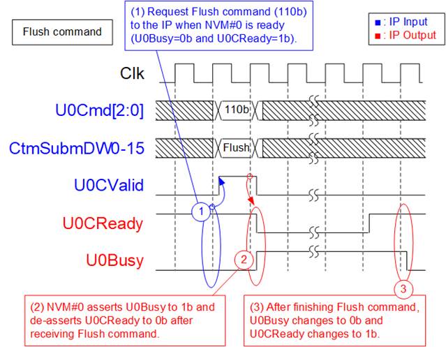
Figure 18: Flush command timing diagram
To execute the SMART command, follow these steps.
1) Ensure that NVM#0 of the IP is ready to receive the command by checking that U0Busy=0b and U0CReady=1b. Then, assert U0CValid with U0Cmd=110b, and set the following values to CtmSubmDW0-DW15 for the Flush command.
CtmSubmDW0 = 0x0000_0000
CtmSubmDW1 = 0x0000_0001
CtmSubmDW2 � CtmSubmDW15 = 0x0000_0000
2) NVM#0 accepts the Flush command by asserting U0Busy to 1b and de-asserting U0CReady to 0b.
3) After the Flush command operation is completed, de-assert U0Busy to 0b, and assert U0CReady to 1b to indicate readiness for the next command.
Note: U0Busy is de-asserted to 0b after U0CReady is asserted for 1 clock cycle to indicate the completion of the operation.
Error

Figure 19: Error flag timing diagram
During the initialization process or while executing certain commands, if an error occurs, the U0Error or U1Error flag is set to 1b. To determine the type of error that occurred, the user can read the U0/U1ErrorType flag. For the User#0 I/F, the user can monitor the error details by checking the value of NVMeCAPReg, U0AdmCompStatus, and U0IOCompStatus after U0Error is asserted to 1b. Similarly, for the User#1 I/F, the user can monitor the error details by checking the value of U1IOCompStatus after U1Error is asserted to 1b.
When encountering an error during the initialization process, it is recommended to read NVMeCAPReg to assess the capabilities of the NVMe SSD. For errors that occur while executing a command, it is recommended to read U0AdmCompStatus or U0/U1IOCompStatus for more detailed information.
- If bit[3] of U0ErrorType is asserted, read U0AdmCompStatus to check more details of the error.
- If bit[5] of U0/U1ErrorType is asserted, read U0/U1IOCompStatus to check more details of the error.
The U0Error and U1Error flag are cleared only by the RstB signal. Once the issue causing the error has been resolved, the user can clear the error flags by asserting RstB to 0b.
Verification Methods
The rmNVMe IP Core for Gen5 functionality was verified by simulation and also proved on real board design by using Agilex7 I-series FPGA Development board.
Recommended Design Experience
Experience design engineers with a knowledge of Quartus Tools should easily integrate this IP into their design.
Ordering Information
This product is available directly from Design Gateway Co., Ltd. Please contact Design Gateway Co., Ltd. For pricing and additional information about this product using the contact information on the front page of this datasheet.
Revision History
|
Revision |
Date |
Description |
|
1.0 |
7-Aug-23 |
New release |