
Design Gateway Co., Ltd
E-mail: ip-sales@design-gateway.com
URL: design-gateway.com
Features
· Function as an NVMe host engine with PCIe Soft IP, enabling direct access to NVMe SSD without requiring a CPU or external memory
· Support two user interfaces (one Write user and one Read user) operating simultaneously
· Support seven commands:
· User#0 (Main user): Identify, Shutdown, Secure Erase, SMART, Flush, and Read
· User#1 (Sub user): Write
· Support multiple Write and Read commands with 4 KB random access
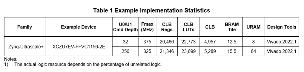
· Configurable command depth of Write and Read independently: 32, 64, 128, or 256 entries
· Buffer size scales with command depth: from 128 KB (32 commands) up to 1 MB (256 commands)
· Provide a simple user interface via Data Stream interface
· Supported NVMe device specifications:
· PCIe I/F: 4-lane PCIe Gen4 (16.0GT/s)
· Base Class Code: 01h (Mass Storage)
· Sub Class Code: 08h (Non-Volatile Memory)
· Programming Interface: 02h (NVMHCI)
· Memory Page Size Minimum (MPSMIN): 0 (4 KB)
· Maximum Queue Entries Supported (MQES): greater than or equal to (2 x Command Depth -1)
· LBA size: 512 bytes
· User clock frequency: At least the PCIe clock frequency (250 MHz for Gen4)
· AMD PCIe PHY IP configuration: 4-lane PCIe Gen4 with 256-bit data interface
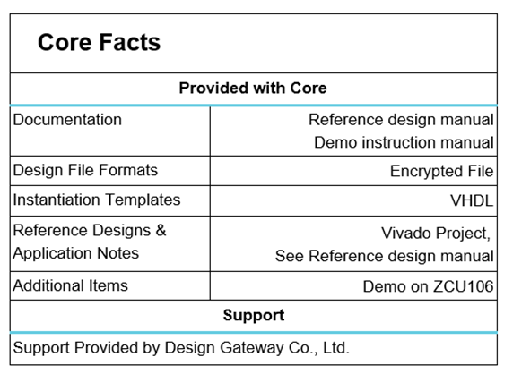
· Available reference design platform: PetaLinux-based demo on ZCU106 with AB17-M2FMC
· Customization services available for additional NVMe commands (e.g., TRIM, Sanitize)
Applications
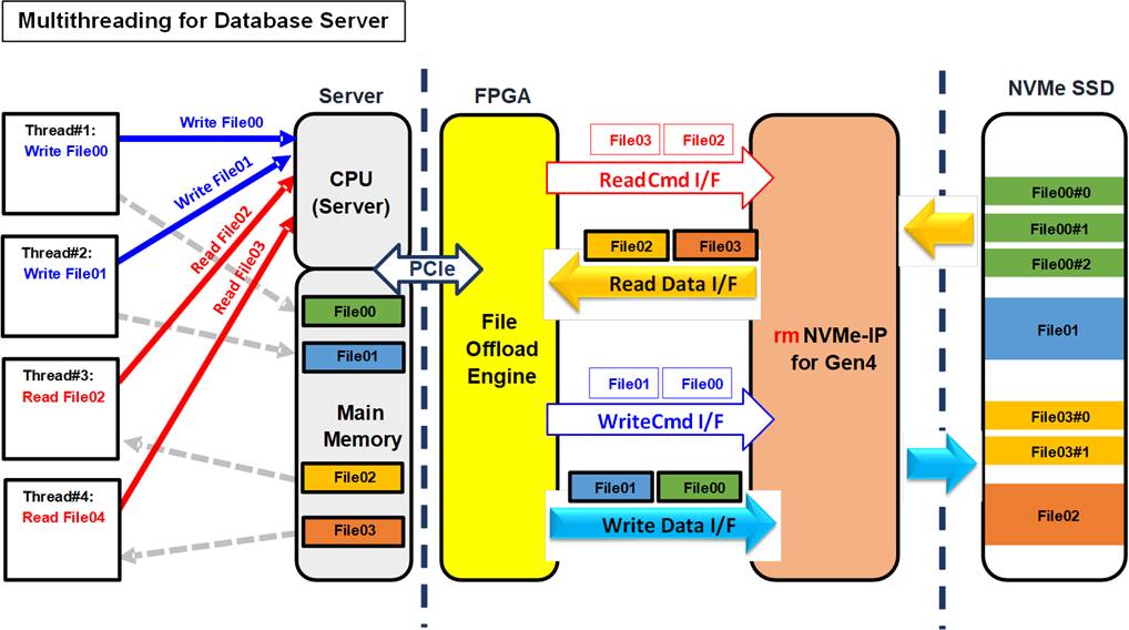
Figure 1 rmNVMeG4-IP Application
The FPGA can be used as an accelerator for a database server to access NVMe SSD storage. In large-scale systems, multiple threads frequently access the database, resulting in a high volume of read and write requests from the CPU. Write data, which is typically large, is buffered in main memory. The FPGA platform, through its PCIe engine, provides an interface that allows the offload engine to receive command requests from the CPU and directly access data in main memory with high performance.
The File Offload Engine issues read and write commands to the rmNVMeG4-IP via the Read Command Interface and Write Command Interface, respectively. Write data is transferred through the Write Data Interface and stored in the NVMe SSD. Read data from the NVMe SSD is returned to the File Offload Engine through the Read Data Interface, and then forwarded to the application threads via main memory.
By utilizing this hardware architecture, database access performance is significantly improved while reducing CPU resource utilization.
General Description
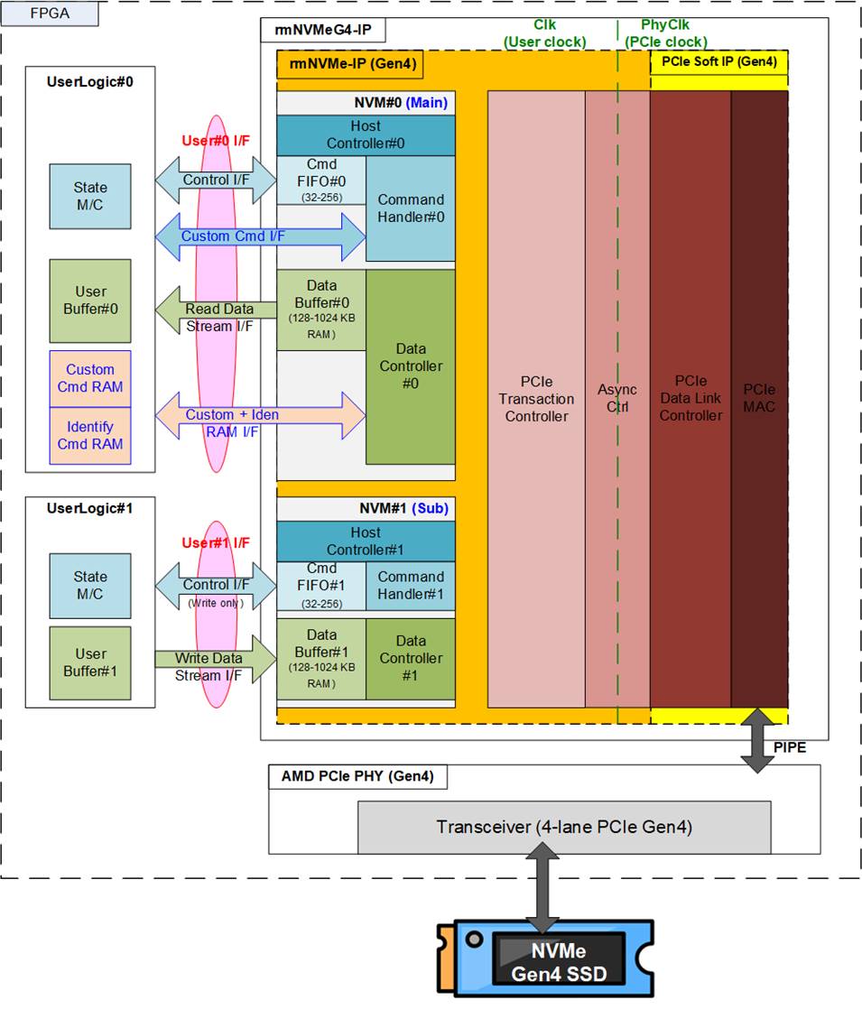
Figure 2 rmNVMeG4-IP Block Diagram
Design Gateway has developed the rmNVMeG4-IP, an NVMe host controller with integrated PCIe Soft IP, enabling direct access to NVMe Gen4 SSD with random access capability and dual-user operation based on the NVM Express standard.
The user interface of the rmNVMe-IP is consistent across both the PCIe Hard IP version (rmNVMe-IP for Gen4) and the PCIe Soft IP version (rmNVMeG4-IP). However, the PCIe interface differs between the two implementations.
In the Hard IP version, the rmNVMe-IP connects to the PCIe Hard IP through a 256-bit AXI4 interface. In contrast, the Soft IP version connects to the AMD PCIe PHY through a 256-bit PIPE. In the Soft IP version, the Data Link layer and part of the Physical layer of the PCIe protocol are implemented within the rmNVMeG4-IP, while the AMD PCIe PHY provides the transceiver and equalization logic.
The rmNVMeG4-IP supports seven NVMe commands: Identify, Shutdown, Write, Read, SMART, Secure Erase, and Flush. These commands are accessed through two user interfaces: User#0 I/F and User#1 I/F. The User#0 I/F corresponds to the NVM#0 module, while the User#1 I/F corresponds to the NVM#1 module. NVM#0 (Main) supports Identify, Shutdown, Read, SMART, Secure Erase, and Flush commands, whereas NVM#1 (Sub) supports only the Write command.
Both User#0 I/F and User#1 I/F consist of two interface groups:
· Control interface for command and parameter transfer
· Data interface for data transfer
The Control interface uses a FIFO-based interface to support multiple Write and Read command requests with parameter configuration. The Data interface for Write and Read commands uses a Data Stream interface with a 256-bit data bus, controlled by valid, ready, and pause signals.
SMART, Secure Erase, and Flush commands require a dedicated Custom Command Interface, which consists of the Ctm I/F for the control path and the Ctm RAM I/F for the data path. The Identify command uses a separate data interface, the Iden RAM I/F. These dedicated interfaces are available only on the User#0 I/F.
With two user interfaces, parallel operation is supported. While the Write command is executed on NVM#1, other commands such as Identify, Read, SMART, and Flush can be processed concurrently on NVM#0. However, Secure Erase and Shutdown commands can only be executed when both NVM#0 and NVM#1 are idle. Therefore, these commands must not be issued while a Write operation is active on NVM#1.
If abnormal conditions occur during initialization or command execution, the rmNVMeG4-IP asserts an error signal. The error status can be read from the IP for further diagnosis. After resolving the issue, both the rmNVMeG4-IP and the NVMe SSD must be reset before resuming operation.
To ensure continuous data transfer on the AMD PCIe PHY interface, the user logic clock frequency must be at least equal to the PHY clock frequency (250 MHz for Gen4). This ensures that the user interface bandwidth is equal to or greater than the PCIe PHY bandwidth, allowing the data stream output to the AMD PCIe PHY to remain valid throughout the entire frame transmission.
Overall, the rmNVMeG4-IP provides a comprehensive solution for high-performance NVMe SSD access. The IP core is supported by reference designs on FPGA evaluation boards, allowing users to evaluate functionality and performance prior to deployment.
Functional Description
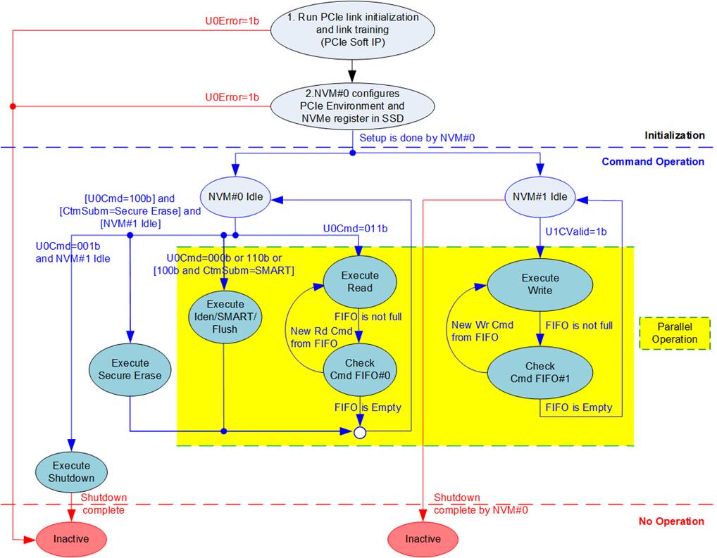
Figure 3 rmNVMeG4-IP Operation Flow
The operation flow of the rmNVMeG4-IP can be divided into three phases: Initialization, Command Operation, and No Operation, as shown in Figure 3.
During the Initialization phase, NVM#0 is responsible for handling the process, while NVM#1 remains idle until initialization is completed. The Initialization phase consists of the following steps:
1) The IP performs PCIe link initialization and training at 4-lane PCIe Gen4 speed. The equalizer parameters are adjusted to ensure optimal signal quality, and flow control parameters are configured. Once the process is completed without any errors, the IP is ready for transferring PCIe packets.
2) NVM#0 initializes the system by configuring PCIe and NVMe registers. If any errors are detected during this process, NVM#0 transitions the IP to the Inactive state.
After the Initialization phase is completed, both user interfaces enter the Idle state and are ready to receive commands. Commands can be issued through both User#0 I/F and User#1 I/F simultaneously. Multiple Read commands (via NVM#0) and multiple Write commands (via NVM#1) can be requested until their respective Cmd FIFOs are full.
However, Secure Erase and Shutdown commands require both NVM#0 and NVM#1 to be in the Idle state before being issued through the User#0 I/F. During Secure Erase operation, NVM#1 must not execute any Write commands. After the Shutdown command is completed, both NVM#0 and NVM#1 transition to the Inactive state.
For a detailed description of each command operation flow during the Command Operation phase of NVM#0 and NVM#1, refer to Figure 4. The left side illustrates the operation of NVM#0, which supports six commands, while the right side illustrates the operation of NVM#1, which supports only the Write command.
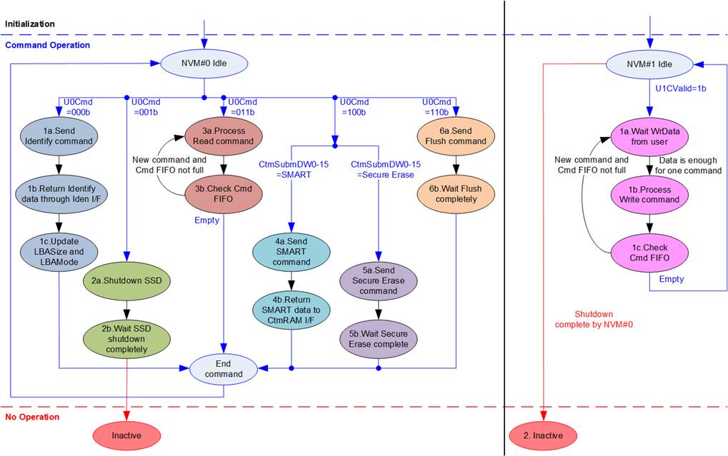
Figure 4 Command Operation Flow of NVM#0 and NVM#1
NVM#0 Operation Flow
1) The first command issued by the user must be the Identify command (U0Cmd=000b) to update the LBASize (disk capacity).
2) The last command before powering down the system must be the Shutdown command (U0Cmd=001b). This command ensures that the SSD is powered down in a proper sequence and all write data is committed to flash memory rather than remaining in the SSD cache. After execution, both the rmNVMeG4-IP and the SSD enter the Inactive state and will not accept further commands until the IP is reset.
3) Each Read command requested to NVM#0 (U0Cmd=011b) has a fixed data size of 4 KB. Multiple Read commands can be issued until Cmd FIFO#0 is full. Steps (3a)–(3b) are repeated until all Read commands are completed.
a) The IP sends a Read command to the SSD.
b) The 4 KB data for each Read command is returned to the user in the same order as the command requests. After each transfer is completed, the corresponding Read command is removed from Cmd FIFO#0, allowing a new command to be issued if the Cmd FIFO is not full. If additional commands are present in the Cmd FIFO, the IP continues processing the next command. Once all data has been transferred and the Cmd FIFO is empty, the IP returns to the Idle state.
4) For the SMART command (U0Cmd=100b and CtmSubmDW0-15=SMART), 512-byte data is returned after completion.
a) The IP issues a Get Log Page command to retrieve SMART/Health information from the SSD.
b) A 512-byte data block is returned from the SSD and forwarded through the Custom command RAM interface.
5) For the Secure Erase command (U0Cmd=100b and CtmSubmDW0-15=Secure Erase), no data is transferred during the operation.
a) The IP issues a Secure Erase command to the SSD.
b) The IP waits for the completion status from the SSD.
6) For the Flush command (U0Cmd=110b), no data is transferred during the operation.
a) The IP issues a Flush command to the SSD.
b) The IP waits for the completion status from the SSD.
NVM#1 Operation Flow
a) The IP waits until a 4 KB Write data block is provided by the user.
b) The IP issues a Write command to the SSD.
c) After the SSD returns a successful completion status, the corresponding Write command is removed from Cmd FIFO#1. A new Write command can be issued if the Cmd FIFO is not full. If additional commands are present, NVM#1 continues processing from step (1a). Once all Write commands are completed and the Cmd FIFO is empty, the IP returns to the Idle state.
2) After the Shutdown command is completed by NVM#0, both the rmNVMeG4-IP and the SSD enter the Inactive state and do not accept new commands until the IP is reset.
Hardware Details
As shown in Figure 2, the rmNVMeG4-IP block diagram consists of multiple submodules. Based on protocol functionality, these submodules are divided into two groups: NVMe for handling the NVMe protocol and PCIe for handling the PCIe protocol. Further details of each submodule are described below.
NVMe
The rmNVMeG4-IP supports seven commands: Identify, Write, Read, SMART, Secure Erase, Flush, and Shutdown. These commands are categorized into two groups: Single-mode commands and Multiple-mode commands.
Single-mode commands include Identify, SMART, Secure Erase, Flush, and Shutdown. These commands are supported exclusively by NVM#0 through the User#0 I/F. When a Single-mode command is issued via Cmd FIFO#0, the command ready signal on the User#0 I/F is de-asserted, preventing additional command requests until the current command has completed.
Multiple-mode commands include Read and Write. The maximum number of outstanding Read commands issued to NVM#0 is determined by the User#0 Command Depth parameter, while the maximum number of outstanding Write commands issued to NVM#1 is determined by the User#1 Command Depth parameter.
The data transfer order on the Data Stream I/F follows the same order as the corresponding Write and Read commands issued through the Cmd FIFO (Control I/F). Each Write and Read command has a fixed transfer size of 4 KB. Therefore, the data buffer size for NVM#0 and NVM#1 is calculated as 4 KB multiplied by the configured command depth. For example, a 128 KB buffer supports 32 commands, while a 1 MB buffer supports 256 commands.
To implement the NVMe protocol, both NVM#0 and NVM#1 consist of five main submodules: Host Controller, Cmd FIFO, Command Handler, Data Buffer, and Data Controller. However, the functionality and complexity of these submodules differ between NVM#0 and NVM#1 due to differences in supported commands.
Further details of each submodule are described in the following sections.
· Host Controller
The Host Controller is the core engine of the rmNVMeG4-IP and is implemented within each NVM module. Its operation is divided into two phases: Initialization and Command Operation.
During the Initialization phase, which occurs once after system boot, the Host Controller configures NVMe registers within the SSD. This process is performed only by Host Controller#0, as illustrated in Figure 3. After initialization is completed, the system transitions to the Command Operation phase.
During command execution, the Host Controller manages the Command Handler. For commands involving data transfer, such as Write, Read, SMART, and Identify, it also controls the Data Controller. The Host Controller monitors the sequence of packets returned from the SSD and decodes status information to determine whether each command has completed successfully or if any errors have occurred. If an error is detected, the corresponding error status is reported to the user.
· Cmd FIFO
The Command FIFO (Cmd FIFO) defines the maximum number of Multiple-mode commands through the Command Depth parameters (U0CDep and U1CDep), as shown in Table 3. The supported command depth values are 32, 64, 128, and 256, which determine the depth of Cmd FIFO#0 and Cmd FIFO#1 in the rmNVMeG4-IP.
Cmd FIFO#0 stores parameters for Read commands, while Cmd FIFO#1 stores parameters for Write commands, enabling Multiple-mode command operations. For Single-mode commands issued to NVM#0, the user must ensure that Cmd FIFO#0 is empty before issuing the command.
· Command Handler
The Command Handler is responsible for generating command packets and decoding completion status packets returned from the SSD. For Identify, Shutdown, Write, and Read commands, command parameters are configured through internal registers. For SMART, Secure Erase, and Flush commands, parameters are provided through a 512-bit Custom Command Interface, defined as a submission queue entry consisting of 16 DWORDs (1 DWORD = 32 bits).
Command completion status is returned through a Completion Queue Entry. The Command Handler provides three types of status outputs for user monitoring:
· 16-bit Admin completion status for Identify and Shutdown commands
· 32-bit I/O completion status for Write and Read commands
· 128-bit Custom completion status (4 DWORDs) for SMART, Secure Erase, and Flush commands
· Data Buffer
Table 2 Command Depth vs Data Buffer Size
|
U0CDep/U1CDep |
Command Depth |
Data Buffer Size |
|
5 |
32 |
128 KB |
|
6 |
64 |
256 KB |
|
7 |
128 |
512 KB |
|
8 |
256 |
1 MB |
· Data Controller
The Data Controller module is responsible for data transfer operations for Identify, SMART, Write, and Read commands. It interfaces with the SSD through three data paths: the Data Stream interface for Write and Read commands, the Custom Command RAM interface for SMART commands, and the Identify interface for Identify commands.
For each Write and Read command, the Data Controller allocates a fixed data size of 4 KB. It also ensures that the data transfer order between the user and the Data Buffer matches the order of the corresponding Write and Read commands issued by the user.
PCIe
PCIe is a high-speed, low-level protocol that serves as the transport layer for NVMe. The NVMe layer operates only after PCIe link initialization is completed. To support the PCIe protocol, the rmNVMeG4-IP includes four main modules: PCIe Transaction Controller, AsyncCtrl, PCIe Data Link Controller, and PCIe MAC. Further details of each module are described below.
· PCIe Transaction Controller
This module implements the Transaction Layer of the PCIe protocol. It converts NVMe commands and data into Transaction Layer Packets (TLPs) for transmission over PCIe. Conversely, received TLPs are decoded and forwarded to the NVMe layer logic.
· AsyncCtrl
The AsyncCtrl module handles clock domain crossing between the NVMe logic and the PCIe PHY. It includes asynchronous registers and buffers to ensure reliable data transfer between clock domains.
Most logic within the rmNVMeG4-IP operates in the user clock domain, while the PCIe PHY operates in the PCIe clock domain. To maintain continuous data transmission, the user clock frequency must be at least equal to the PCIe PHY clock frequency.
· PCIe Data Link Controller
This module implements the Data Link Layer of the PCIe protocol, ensuring reliable delivery of TLPs between the Transaction Controller and the PCIe interface. Each TLP is appended with a Link Cyclic Redundancy Code (LCRC) for error detection. A sequence number is also included to maintain packet ordering and detect missing packets.
Upon successful reception and validation, an Acknowledge Data Link Layer Packet (ACK DLLP) is generated to confirm correct delivery. If an error is detected, a Negative Acknowledge (NAK DLLP) is issued, prompting retransmission of the affected TLPs.
The PCIe Soft IP also includes two 4 KB RAM blocks used as a replay buffer and a data buffer for bidirectional data transfer.
· PCIe Media Access Controller (PCIe MAC)
The PCIe MAC interfaces with the AMD PCIe PHY through the PIPE (PHY Interface for PCI Express) standard. It performs two primary functions: link initialization and training, and packet transmission control in accordance with PCIe physical layer specifications.
During link initialization and training, certain functions are handled by the AMD PCIe PHY, including Clock and Data Recovery (CDR) for bit lock and block alignment at Gen4 speed. The PCIe MAC implements the Link Training and Status State Machine (LTSSM), which controls link width, lane reversal, polarity inversion, and link speed. Due to the high data rate of Gen4 (16.0 GT/s), additional mechanisms such as DC balance and equalization are applied to ensure signal integrity and optimal performance.
After link initialization is completed, data transmission begins. On the transmit side, the PCIe MAC performs functions such as data multiplexing, byte striping across lanes, and data scrambling to reduce electromagnetic interference. On the receive side, it performs data descrambling, byte un-striping, and filtering to reconstruct the original data stream.
User Logic
The User Logic can be implemented using a simple state machine to issue commands and configure parameters for each operation. With support for multiple Write and Read commands, users can send command requests through the Control interface (Cmd FIFO) and transfer data independently through the Data Stream interface using valid and ready signals.
The output data from SMART and Identify commands can be mapped to a simple dual-port RAM with byte-enable support. All data interfaces use a 256-bit data width. The Identify command returns 8 KB of data, while the SMART command returns 512 bytes.
AMD PCI Express PHY
AMD provides the PCI Express PHY to enable the use of Soft IP for implementing a PCIe MAC, eliminating the need for PCIe Hard IP. The PCIe PHY uses the PIPE (PHY Interface for PCI Express) standard as its user interface. When operating with the rmNVMeG4-IP, the PCIe PHY is configured for 4 lanes with a link speed of 16.0 GT/s (PCIe Gen4).
For more detailed information on the AMD PCIe PHY, refer to the PG239: PCI Express PHY documentation available on the AMD website:
https://docs.amd.com/r/en-US/pg239-pcie-phy
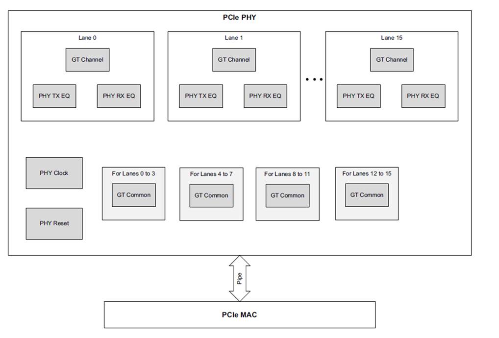
Figure 5 Block Diagram of the PCI Express PHY
Core I/O Signals
Table 3 provides detailed descriptions of configurable parameters, while Table 4 and Table 5 outline the I/O signals for rmNVMeG4-IP.
Table 3 Core Parameters
|
Name |
Value |
Description |
|
U0CDep |
5-8 |
Command queue depth configuration for NVM#0. Valid values range from 5 to 8. The command queue depth is equal to 2U0CDep, as described in Table 2. |
|
U1CDep |
5-8 |
Command queue depth configuration for NVM#1. This parameter has the same function as U0CDep but applies to NVM#1. |
Table 4 User I/O Signals (Synchronous to Clk)
|
Signal name |
Dir |
Description |
|
Control I/F of rmNVMeG4-IP |
||
|
RstB |
In |
Synchronous reset, active low. This signal must be de-asserted to 1b when the Clk signal is stable. |
|
Clk |
In |
User clock for operating the rmNVMeG4-IP. The clock frequency must be greater than or equal to the PCIeClk frequency (clock output from the PCIe Hard IP). For 4-lane PCIe Gen4, PCIeClk is 250 MHz. |
|
U0Cmd[2:0] |
In |
Command input for User#0 I/F. Valid when U0CValid=1b. 000b: Identify, 001b: Shutdown, 011b: Read SSD, 100b: SMART/Secure Erase, 110b: Flush, Others: Reserved While NVM#0 is busy (U0Busy = 1b), only Read commands can be issued. All other commands can be issued only when U0Busy = 0b. |
|
U0Addr [47:0] |
In |
Start address for User#0 Read commands, in units of 512 bytes. Valid when U0CValid=1b. This value must be less than the SSD capacity (LBASize). Note: U0Addr[2:0] are ignored for 4 KB alignment. |
|
U0CValid |
In |
Command valid. Assert to 1b to issue a new command to NVM#0. For Single-mode commands (Identify, Shutdown, SMART, Secure Erase, and Flush), U0CReady is de-asserted to 0b after U0CValid is asserted. For Read commands, additional commands can be issued while U0CReady remains asserted to 1b. |
|
U0CReady |
Out |
Asserted to 1b to indicate that NVM#0 is ready to accept a new command. |
|
U0Busy |
Out |
Busy status of User#0 I/F. Asserted to 1b when NVM#0 is processing a command. |
|
U0CCnt[8:0] |
Out |
Number of Read commands currently stored in Cmd FIFO#0. The value ranges from 0 to User#0 Command Depth. This signal is ignored for Single-mode commands. Example: If Command Depth = 32, valid range is 0 to 32. |
|
U0CId[7:0] |
Out |
Command ID for Read commands in Cmd FIFO#0. Valid when U0CValid = 1b. The value ranges from 0 to (User#0 Command Depth – 1). It is used to match with · U0DId for tracking data stream transferred via the Read Data Stream interface of User#0 I/F · Error ID of U0IOCompStatus[23:16] Ignored for Single-mode commands. Example: If Command Depth = 32, valid range is 0 to 31. |
|
U1Addr[47:0] |
In |
Start address for User#1 Write commands, in units of 512 bytes. Valid when U1CValid = 1b. The address must be less than the SSD capacity (LBASize). Note: U1Addr[2:0] are ignored for 4 KB alignment. |
|
U1CValid |
In |
Command valid. Assert to 1b to issue a new Write command to NVM#1. Additional Write commands can be issued while U1CReady remains asserted to 1b. |
|
U1CReady |
Out |
Asserted to 1b to indicate that NVM#1 is ready to accept a Write command. |
|
U1Busy |
Out |
Busy status of User#1 I/F. Asserted to 1b when NVM#1 is processing a command. |
|
U1CCnt[8:0] |
Out |
Number of Write commands currently stored in Cmd FIFO#1. The value ranges from 0 to User#1 Command Depth. Example: If Command Depth = 32, valid range is 0 to 32. |
|
U1CId[7:0] |
Out |
Command ID for Write commands in Cmd FIFO#1. Valid when U1CValid = 1b. The value ranges from 0 to (User#1 Command Depth – 1). It is used to match with · U1DId for tracking data stream transferred via the Write Data Stream interface of User#1 I/F · Error ID of U1IOCompStatus[23:16] Example: If Command Depth = 32, valid range is 0 to 31. |
|
LBASize[47:0] |
Out |
Total SSD capacity in units of 512 bytes, aligned to 4 KB. Valid after completion of the Identify command. |
|
Signal name |
Dir |
Description |
|
U0-1Error |
Out |
Error indicator. Asserted to 1b when
either U0ErrorType or U1ErrorType is not equal to 0. |
|
U0ErrorType[31:0] |
Out |
Error status of User#0. [0] – An error when PCIe class code is incorrect. [1] – An error from Controller capabilities (CAP) register, which can occur due to various reasons. - Memory Page Size Minimum (MPSMIN) is not equal to 0. - NVM command set flag (bit 37 of CAP register) is not set to 1. - Doorbell Stride (DSTRD) is not equal to 0. - Maximum Queue Entries Supported (MQES) is less than (2 x max<User#0 Command Depth, User#1 Command Depth> - 1). [2] – An error when the Admin completion entry is not received within the specified timeout. [3] – An error when the status register in the Admin completion entry is not 0 or when the phase tag/command ID is invalid. Further information can be found in the AdmCompStatus signal. [4] – An error when the IO completion entry of NVM#0 is not received within the specified timeout. [5] – An error when the status register in the IO completion entry of NVM#0 is not 0 or when the phase tag is invalid. More details are available in the IOCompStatus signal. [6] – An error from unsupported LBA unit where the LBA unit is not equal to 512 bytes. [7] – An error when the number of queues supported by the SSD is less than 2. [8] – An error when the received size of Transaction Layer Packet (TLP) is incorrect. [9] - An error from PCIe PHY IP. Bits[15:10] are mapped to Uncorrectable Error Status Register. [10] – Mapped to Unsupported Request (UR) Status (bit[20]). [11] – Mapped to Completer Abort (CA) Status (bit[15]). [23:12] – Reserved. Bits[30:24] are also mapped to Uncorrectable Error Status Register. [24] – Mapped to Data Link Protocol Error Status (bit[4]). Bits[27:25] – Reserved [28] – Mapped to Uncorrectable Internal Error Status (bit[22]). Bits[31:29] – Reserved Note: Timeout period of bit[2]/[4] is determined by the TimeOutSet input. |
|
U1ErrorType[31:0] |
Out |
Error status of User#1. [3:0] – Reserved. [4] – An error when the IO completion entry of NVM#1 is not received within the specified timeout. [5] – An error when the status register in the IO completion entry of NVM#1 is not 0 or when the phase tag is invalid. More details are available in the IOCompStatus signal. [31:6] – Reserved. Note: Timeout period of bit[4] is determined by the TimeOutSet input. |
|
Data I/F of rmNVMeG4-IP |
||
|
U0DId[7:0] |
In |
Indicate User#0 Command ID (U0CId) corresponding to the data currently being transferred on the Read Data Stream interface during Read commands. Valid when U0RdValid = 1b. The value ranges from 0 to (User#0 Command Depth – 1). |
|
U0RdData[255:0] |
Out |
User#0 Read data returned from the SSD during Read commands. Valid when U0RdValid =1b. |
|
U0RdValid |
Out |
User#0 Read data valid that is asserted to 1b when U0RdData is valid. The user can pause data transmission by asserting U0RdPause to 1b. After that, U0RdValid is de-asserted within 4 clock cycles. |
|
U0RdPause |
In |
Assert to 1b to pause the U0RdData transmission. U0RdValid will be de-asserted within 4 clock cycles. |
|
U1DId[7:0] |
Out |
Indicates the User#1 Command ID (U1CId) corresponding to the data currently being transferred on the Write Data Stream interface during Write commands. Valid when U1WrValid = 1b. The value ranges from 0 to (User#1 Command Depth – 1). |
|
U1WrData[255:0] |
In |
User#1 Write data to SSD during Write commands. Valid when U1WrValid=1b. |
|
U1WrValid |
In |
Write data valid signal for User#1. Assert to 1b to indicate that U1WrData is valid and can be written to NVM#1 during Write commands. Write data can be transferred before issuing the corresponding Write command (U1CValid). |
|
U1WrReady |
Out |
Asserted to 1b when NVM#1 accepts the write data (U1WrData). |
|
U1WrCnt[15:0] |
Out |
Total data count of Write data stored in Data Buffer#1 in 256-bit unit. The value ranges from 0 to 64 times of User#1 Command Depth. |
|
Signal name |
Dir |
Description |
|
rmNVMeG4-IP Interface |
||
|
IPVersion[31:0] |
Out |
IP version number. |
|
U0TestPin[127:0], U1TestPin[15:0] |
Out |
Reserved to be internal IP Test point. |
|
TimeOutSet[31:0] |
In |
Timeout value to wait for completion responses from SSD. The time unit is equal to one clock period (1/ Clk frequency). If TimeOutSet = 0, the timeout function is disabled. |
|
U0AdmCompStatus [15:0] |
Out |
Status output from the Admin Completion Entry. [0] – Set to 1b when the Phase tag or Command ID is invalid. [15:1] – Status field value of Admin Completion Entry |
|
U0IOCompStatus[15:0] |
Out |
Status output from IO Completion Entry of NVM#0. [0] – Set to 1b when the Phase tag is invalid. [15:1] – Status field value of IO Completion Entry [23:16] – Command ID of IO Completion Entry (corresponds to U0Cid) [31:24] – Reserved. |
|
U1IOCompStatus[15:0] |
Out |
Status output from IO Completion Entry of NVM#1 [0] – Set to 1b when the Phase tag is invalid. [15:1] – Status field value of IO Completion Entry [23:16] – Command ID of IO Completion Entry (corresponds to U1Cid) [31:24] – Reserved. |
|
NVMeCAPReg[31:0] |
Out |
NVMe capability register value, when U0ErrorType[1]=1b. [15:0] – Maximum Queue Entries Supported (MQES) [19:16] – Doorbell Stride (DSTRD) [20] – NVM command set flag [24:21] – Memory Page Size Minimum (MPSMIN) [31:25] – Reserved |
|
Identify Interface (RAM) for User#0 |
||
|
IdenWrEn |
Out |
Asserted to 1b to indicate valid output data for the Identify command. |
|
IdenWrDWEn[7:0] |
Out |
Dword (32-bit) enable of IdenWrData. Valid when IdenWrEn=1b. 1b: Corresponding Dword data is valid, 0b: Corresponding Dword data is not valid. Bit[0], [1], …, [7] correspond to IdenWrData[31:0], [63:32], …, [255:224], respectively |
|
IdenWrAddr[7:0] |
Out |
Index of IdenWrData in 256-bit unit. Valid when IdenWrEn=1b. 00h-7Fh: 4 KB Identify Controller data, 80h-FFh: 4 KB Identify Namespace data. |
|
IdenWrData[255:0] |
Out |
4 KB Identify Controller data or Identify Namespace data. Valid when IdenWrEn=1b. |
|
Custom interface (Command and RAM) for User#0 |
||
|
CtmSubmDW0[31:0] – CtmSubmDW15[31:0] |
In |
16 Dwords of Submission queue entry for SMART, Secure Erase, or Flush command. DW0: Command Dword0, DW1: Command Dword1, …, and DW15: Command Dword15. Valid when U0CValid=1b and U0Cmd=100b (SMART/Secure Erase) or 110b (Flush). |
|
CtmCompDW0[31:0] – CtmCompDW3[31:0] |
Out |
4 Dwords of Completion queue entry, output from SMART, Secure Erase, or Flush command. DW0: Completion Dword0, DW1: Completion Dword1, …, and DW3: Completion Dword3 |
|
CtmRamWrEn |
Out |
Asserted to 1b to indicate valid output data from Custom commands (e.g., SMART). |
|
CtmRamWrDWEn[7:0] |
Out |
Dword (32-bit) enable of CtmRamWrData. Valid when CtmRamWrEn=1b. 1b: Corresponding Dword data is valid, 0b: Corresponding Dword data is not valid. Bit[0], [1], …, [7] correspond to CtmRamWrData[31:0], [63:32], …, [255:224], respectively. |
|
CtmRamAddr[7:0] |
Out |
Index of CtmRamWrData when SMART data is received. Valid when CtmRamWrEn=1b. (Optional) Used as an index for reading input data from CtmRamRdData for customized Custom commands. |
|
CtmRamWrData[255:0] |
Out |
512-byte data output from SMART command. Valid when CtmRamWrEn=1b. |
|
CtmRamRdData[255:0] |
In |
(Optional) Data input for customized Custom commands. |
Table 5 Physical I/O Signals for PCIe4C/PL PCIE4 (Synchronous to PhyClk)
|
Signal name |
Dir |
Description |
|
PHY System Signal |
||
|
PCIeRstB |
In |
Synchronous reset signal. Active low. De-assert to 1b when PCIe PHY IP is not in reset state, detected by phy_phystatus_rst signal being de-asserted to 0b. |
|
PhyClk |
In |
Clock output from PCIe Hard IP (250 MHz for 4-lane PCIe Gen4). |
|
Others PHY Interface |
||
|
MACTestPin[127:0] |
Out |
Test point of PCIe MAC. |
|
MACStatus[7:0] |
Out |
Status output from PCIe MAC. [5:0] – LTSSM - 000000b: Detect.Quiet - 000001b: Detect.Active - 000010b: Polling.Active - 000011b: Polling.Configuration - 000100b: Config.Linkwidth - 000101b: Config.Lanenum - 000110b: Config.Complete - 000111b: Config.Idle - 001000b: Recovery.RcvrLock - 001001b: Recovery.Speed - 001010b: Recovery.RcvrCfg - 001011b: Recovery.Idle - 010000b: L0 - 100000b: Recovery.EqP0 - 100001b: Recovery.EqP1 - 100010b: Recovery.EqP2 - 100011b: Recovery.EqP3 [6] – Reserved [7] – Asserted to 1b after PCIe initialization is completed. |
|
PIPE Data Interface |
||
|
PhyTxData[255:0] |
Out |
Parallel data output to PHY. |
|
PhyTxDataK[7:0] |
Out |
Control data to indicate whether PCIeTxData is control or data. |
|
PhyTxDataValid[3:0] |
Out |
Asserted to 1b when the valid data is presented on PhyTxData. |
|
PhyTxStartBlock[3:0] |
Out |
Asserted to 1b at the first clock of 128b block to indicate the start of block. Valid when PhyTxDataValid=1b. |
|
PhyTxSyncHeader[7:0] |
Out |
Indicate whether data block is ordered set or data stream. Valid at the first clock of 128b block, together with PhyTxStartBlock. |
|
PhyRxData[255:0] |
In |
Data input from PHY. |
|
PhyRxDataK[7:0] |
In |
Control data to indicate whether PhyRxData is control or data. |
|
PhyRxDataValid[3:0] |
In |
Asserts to 1b when the valid data is presented on PhyRxData. |
|
PhyRxStartBlock[7:0] |
In |
Asserts to 1b at the first clock of 128b block to indicate the start of block. Valid when PhyRxDataValid=1b. |
|
PhyRxSyncHeader[7:0] |
In |
Indicates whether data block is ordered set or data stream. Valid at the first clock of 128b block, together with PhyRxStartBlock. |
|
PIPE Control and Status Signal |
||
|
PhyTxDetectRx |
Out |
Requests PCIe PHY to begin a receiver detection operation. |
|
PhyTxElecIdle[3:0] |
Out |
Forces Tx to enter electrical idle state. |
|
PhyTxCompliance[3:0] |
Out |
Asserted to 1b for running negative disparity. |
|
PhyRxPolarity[3:0] |
Out |
Requests PCIe PHY to perform polarity inversion on the received data. |
|
PhyPowerdown[1:0] |
Out |
Requests PCIe PHY to change the power state. |
|
PhyRate[1:0] |
Out |
Requests PCIe PHY to change link rate. |
|
PhyRxValid[3:0] |
In |
Indicates symbol lock and valid data when logic high. |
|
PhyPhyStatus[3:0] |
In |
Used to communicate completion of several PIPE operations. |
|
PhyRxElecIdle[3:0] |
In |
Indicates Rx electrical idle detected. |
|
PhyRxStatus[11:0] |
In |
Rx status and error codes. |
|
Signal name |
Dir |
Description |
|
Driver and Equalization Signal |
||
|
PhyTxMargin[2:0] |
Out |
Selects Tx voltage levels. This signal is fixed to 000b. |
|
PhyTxSwing |
Out |
Controls Tx voltage swing level. This signal is fixed to 0b. |
|
PhyTxDeEmph |
Out |
Selects Tx de-emphasis. This signal is fixed to 1b. |
|
PhyTxEqCtrl[7:0] |
Out |
Tx equalization control. |
|
PhyTxEqPreset[15:0] |
Out |
Tx equalization preset. |
|
PhyTxEqCoeff[23:0] |
Out |
Tx equalization coefficient. |
|
PhyTxEqFS[5:0] |
In |
Indicates the full swing of the Tx driver. Static value based on characteristics of Tx driver. |
|
PhyTxEqLF[5:0] |
In |
Indicates the low frequency of the Tx driver. Static value based on characteristics of Tx driver. |
|
PhyTxEqNewCoeff[71:0] |
In |
Status of the current Tx equalization coefficient. |
|
PhyTxEqDone[3:0] |
In |
Asserts to 1b when Tx equalization is done. |
|
PhyRxEqCtrl[7:0] |
Out |
Rx equalization control. |
|
PhyRxEqTxPreset[15:0] |
Out |
Link partner status for Tx preset. |
|
PhyRxEqPresetSel[3:0] |
In |
Serves indications as coefficient or preset. |
|
PhyRxEqNewTxCoeff [71:0] |
In |
New Tx coefficient or preset to request the link partner. |
|
PhyRxEqAdaptDone[3:0] |
In |
Asserts to 1b when RX equalization is successfully done. Valid when PhyRxEqDone is asserted to 1b. |
|
PhyRxEqDone[3:0] |
In |
Asserts to 1b when Rx equalization is finished. |
|
Assist Signal |
||
|
AsMacInDetect |
Out |
Assists PCIe PHY to switch the receiver termination between VTT and GND. |
|
AsCdrHoldReq |
Out |
Assists PCIe PHY to hold CDR. |
Note: For more detailed information about the signals of AMD PCIe PHY, please refer to the “PG239: PCI Express PHY” document, available at AMD website.
Timing Diagram
Initialization
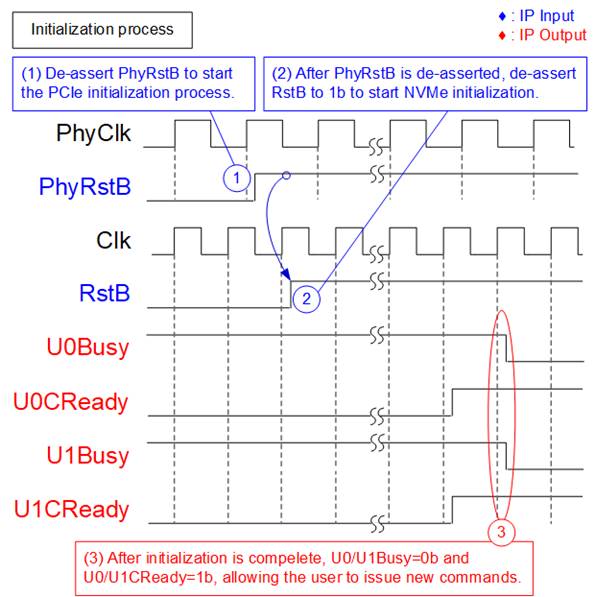
Figure 6 Timing Diagram During Initialization Process
The initialization process of the rmNVMeG4-IP follows the steps below, as shown in the timing diagram.
1) Monitor the phy_phystatus_rst signal from the PCIe PHY and wait until it is de-asserted to 0b, indicating the completion of the PCIe PHY reset process. After that, the user logic de-asserts PhyRstB to 1b to initiate the link training process by rmNVMeG4-IP.
2) After de-asserting PhyRstB and ensuring the stability of the Clk signal, the user logic can de-assert RstB to 1b. This action triggers the NVMe initialization within the rmNVMeG4-IP.
3) Once the rmNVMeG4-IP completes all initialization processes, including link training, flow control initialization, and configuration of PCIe and NVMe registers, the IP de-asserts U0Busy and U1Busy to 0b. At the same time, U0CReady and U1CReady are asserted to 1b, indicating readiness to receive new commands from the user.
After completing all of the above steps, the rmNVMeG4-IP is ready to receive commands from the user.
Control Interface (Single Mode)
The rmNVMeG4-IP supports two command types: Single-mode and Multiple-mode. Single-mode commands are handled exclusively through the User#0 I/F, while the User#1 I/F supports only the Write command (a Multiple-mode command).
To initiate a Single-mode command, NVM#0 must be in the Idle state (U0Busy=0b and U0CReady=1b). During the execution of a Single-mode command, the User#0 I/F cannot accept new command requests until the ongoing Single-mode command operation is completed.
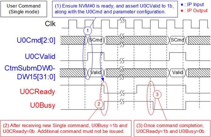
Figure 7 Single-Mode Command Timing Diagram (User#0 I/F)
Figure 7 shows timing diagram for executing Single-mode commands (Identify, Shutdown, SMART, Secure Erase, and Flush) in NVM#0.
1) Before issuing a new command to NVM#0, the user must verify that U0Busy=0b and U0CReady=1b to ensure that NVM#0 is in an Idle state. Subsequently, U0CValid is asserted to 1b for one clock cycle along with a valid U0Cmd and the required command-specific parameters.
Note: SMART, Secure Erase, and Flush commands require the parameters CtmSubmDW0-DW15. Identify and Shutdown commands do not require any parameters
2) Upon receiving the new command request, NVM#0 asserts U0Busy to 1b and initiates the command operation. Simultaneously, U0CReady is de-asserted to 0b to prevent additional command requests.
3) After completing the command operation, U0Busy is de-asserted to 0b, and U0CReady is re-asserted to 1b, indicating that the interface is ready for the next command.
In the case of a Shutdown command, after completion, both U0Busy and U0CReady remain de-asserted to 0b, preventing any further command requests until the IP is reset.
Note: For Single-mode commands, U0CReady may be asserted for one clock cycle to acknowledge the command request, followed by U0Busy being de-asserted to 0b to indicate the command completion. The user should issue the next command only after U0Busy = 0b.
Control Interface (Multiple Mode)
The Control interface of the rmNVMeG4-IP supports two Multiple-mode commands: Read command by User#0 I/F and Write command by User#1 I/F.
Unlike Single-mode commands, multiple command requests can be issued by asserting U0CValid or U1CValid to 1b when U0CReady or U1CReady is asserted to 1b. There is no requirement to wait for U0Busy or U1Busy to be de-asserted to 0b. The maximum number of Read and Write commands can be configured independently using U0CDep and U1CDep. The Control interface operation is described below.
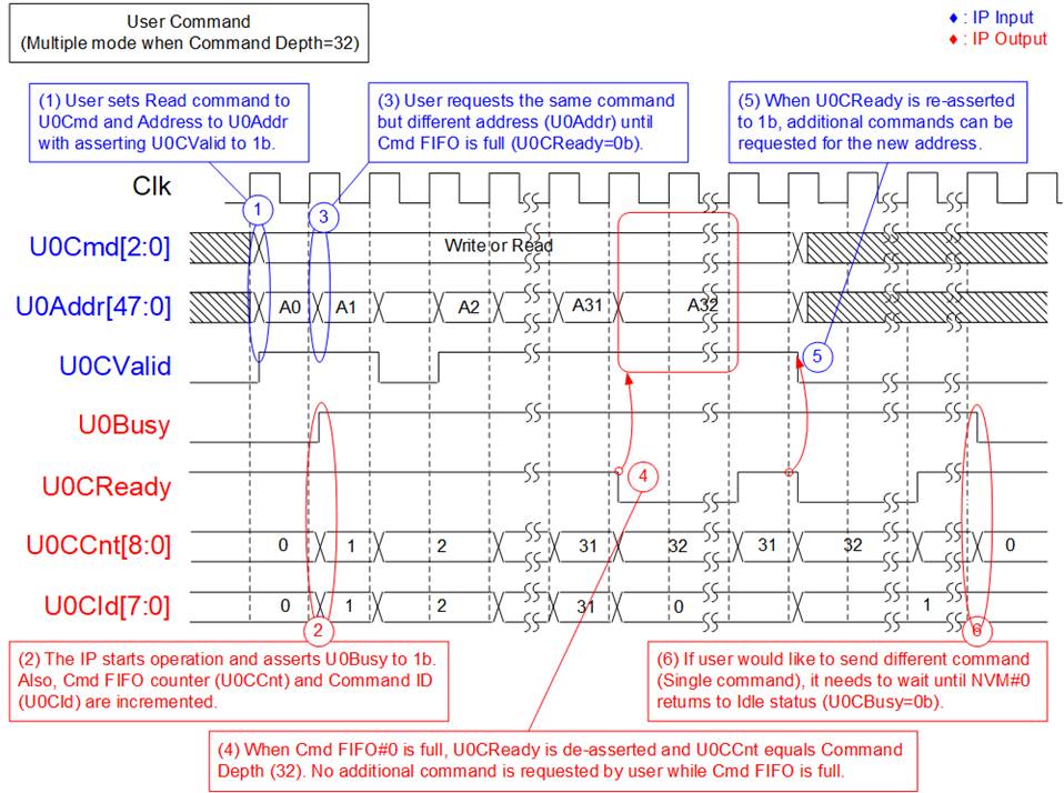
Figure 8 Multiple-Mode Command Timing Diagram (User#0 I/F)
Since the timing for issuing Read commands on the User#0 I/F and Write commands on the User#1 I/F is similar, Figure 8 illustrates the User#0 I/F timing when NVM#0 executes Read commands with U0CDep = 5 (maximum 32 commands).
1) If the previous command is not a Read command, the user must ensure that NVM#0 is idle (U0Busy=0b) and Cmd FIFO#0 is ready (U0CReady=1b). Next, the user sends a Read command (U0Cmd=011b) to NVM#0 by asserting U0CValid to 1b for one clock cycle, along with the valid U0Addr.
2) NVM#0 initiates the command operation by asserting U0Busy to 1b. Meanwhile, U0CCnt and U0CId are incremented to indicate the number of commands in Cmd FIFO#0 and the next command ID, respectively.
3) As long as Cmd FIFO#0 is not full (U0CCnt is less than the configured Command Depth (32) or U0CReady=1b), the user can continue issuing Read commands with new address values. While NVM#0 is busy (U0Busy = 1b), U0Cmd must be assigned to the Read command. Assigning any other command during this time results in undefined behavior.
4) When Cmd FIFO#0 becomes full (U0CCnt = User#0 Command Depth), U0CReady is de-asserted to 0b, and no further command requests are accepted. All inputs for the new command request must retain the same value until U0CReady is re-asserted.
5) After some commands are completed and Cmd FIFO#0 is not full (U0CCnt < User#0 Command Depth), U0CReady is re-asserted, allowing new command requests to be accepted.
6) When all pending Read commands are completed, U0Busy is de-asserted to 0b, and NVM#0 returns to the Idle state. At this point, NVM#0 can accept new commands, including Single-mode commands.
Note: The User#1 I/F supports only the Write command. Therefore, the U1Cmd signal is not implemented for NVM#1.
Control Interface (Parallel Command)
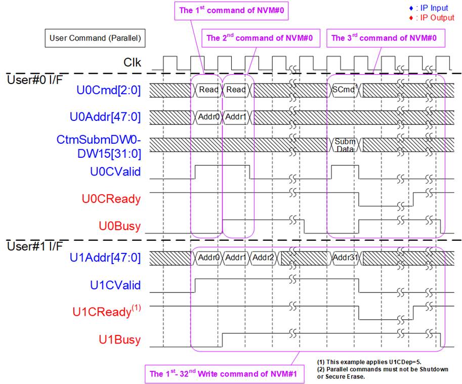
Figure 9 Multiple-Mode Command Timing Diagram (User#0 I/F)
Both User#0 I/F and User#1 I/F provide independent control paths, allowing commands to be executed simultaneously. Figure 9. illustrates the Control interfaces when NVM#0 and NVM#1 operate in parallel.
This enables commands such as Identify, SMART, Flush, and Read in NVM#0 to be executed concurrently with Write commands in NVM#1.
However, Shutdown and Secure Erase commands are exceptions and cannot be executed concurrently with any other commands. These commands require both NVM#0 and NVM#1 to be in the Idle state before execution.
Read Data Stream Interface
The Read Data Stream interface of the rmNVMeG4-IP is available on the User#0 I/F and is used for data transfer during Read commands. This interface uses two control signals: valid (U0RdValid) and pause (U0RdPause).
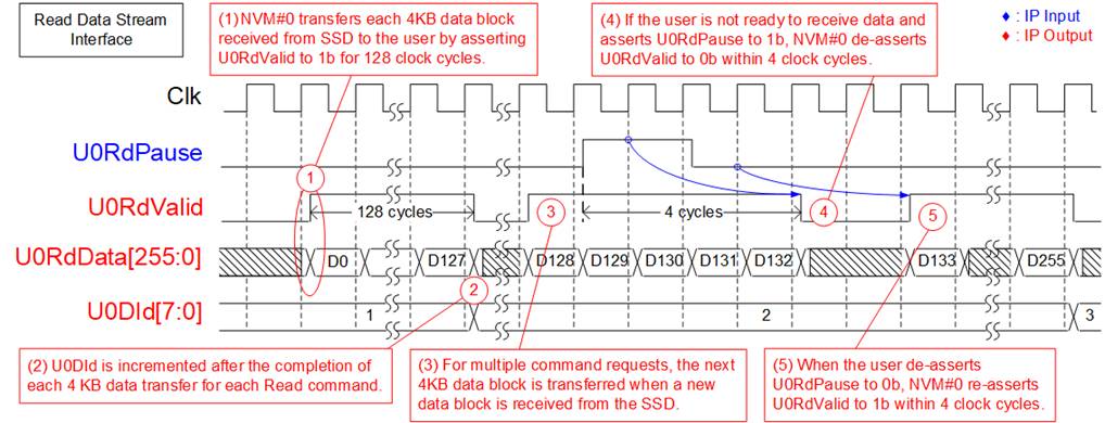
Figure 10 Read Data Stream Interface
1) When NVM#0 receives a 4 KB data block from the SSD for the current command ID, it transfers the data to the user by asserting U0RdValid to 1b along with valid U0RdData. To transfer the full 4 KB data block, U0RdValid remains asserted for 128 consecutive clock cycles, assuming U0RdPause is continuously de-asserted to 0b.
2) After completing the transfer of each 4 KB data block, U0DId is incremented to indicate the command ID of the next data block.
3) The next 4 KB data block is transferred after it is received from the SSD, following the same process as described in step (1).
4) If the user is not ready to receive data, U0RdPause can be asserted to 1b. In response, NVM#0 pauses the data transfer by de-asserting U0RdValid to 0b within 4 clock cycles.
5) When the user is ready to resume data reception, U0RdPause is de-asserted to 0b. NVM#0 then re-asserts U0RdValid to 1b within 4 clock cycles to continue the data transfer.
Note: When the Command Depth is set to 32, U0DId ranges from 0 to 31.
Write Data Stream Interface
The Write Data Stream interface on the User#1 I/F of the rmNVMeG4-IP is responsible for data transfer during Write commands. This interface operates independently from the Control interface, allowing the user to prepare Write data in Data Buffer#1 either before or after issuing the Write command request. Figure 11 illustrates timing diagram of Write commands with User#1 Command Depth configured to 5 (maximum 32 commands).
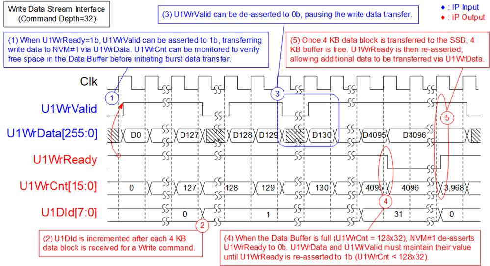
Figure 11 Write Data Stream Interface
1) Before initiating data transfer, the user verifies that NVM#1 is ready to receive data by monitoring U1WrReady=1b or ensuring U1WrCnt < 64xUser#1 Command Depth (2048). Once confirmed, the user asserts U1WrValid along with valid U1WrData to transfer 256-bit data.
Two status signals, U1WrReady and U1WrCnt, serve as flow control signals for the Write command. U1WrCnt is recommended for burst data transfer, while U1WrReady is suitable for non-burst data transfer.
2) After completing the transfer of each 4 KB data block (the size of each Write command), U1DId is incremented to indicate the command ID of the next data block.
3) The user can pause data transfer at any time by de-asserting U1WrValid to 0b.
4) When the Data Buffer#1 becomes full (U1WrCnt reaches 64 x User#1Command Depth or 2048), U1WrReady is de-asserted to 0b and NVM#1 cannot accept additional data. Both U1WrData and U1WrValid must maintain the same value until U1WrReady is re-asserted to 1b.
5) After a Write command completes and 4 KB of buffer space is released, U1WrCnt decreases accordingly. U1WrReady is then re-asserted to 1b , allowing additional data to be transferred.
Data Stream Interface (Parallel Data)
The Data Stream interfaces for Read and Write operations in the rmNVMeG4-IP operate independently on User#0 I/F and User#1 I/F, respectively. The Read Data Stream interface (User#0 I/F) is used to transfer data from NVM#0 to the user during Read commands, while the Write Data Stream interface (User#1 I/F) is used to transfer data from the user to NVM#1 during Write commands.
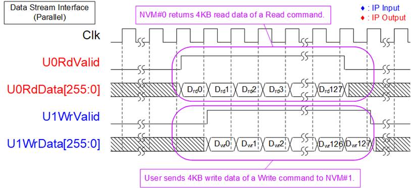
Figure 12 Data Stream Interface When Transferring Read and Write Parallelly
Due to the independent operation of these interfaces, the rmNVMeG4-IP supports parallel data transfer. This enables concurrent Read and Write operations, as shown in Figure 12. While NVM#0 returns Read data to the user, the user can simultaneously send Write data to NVM#1 without interference.
IdenCtrl/IdenName
To ensure proper operation of the system, it is recommended to send the Identify command to the IP as the first command after the system boots up. This command updates SSD total capacity (LBASize) which is necessary for Write and Read commands to operate correctly. The address (U0Addr/U1Addr) must not exceed the total capacity (LBASize) of the SSD.
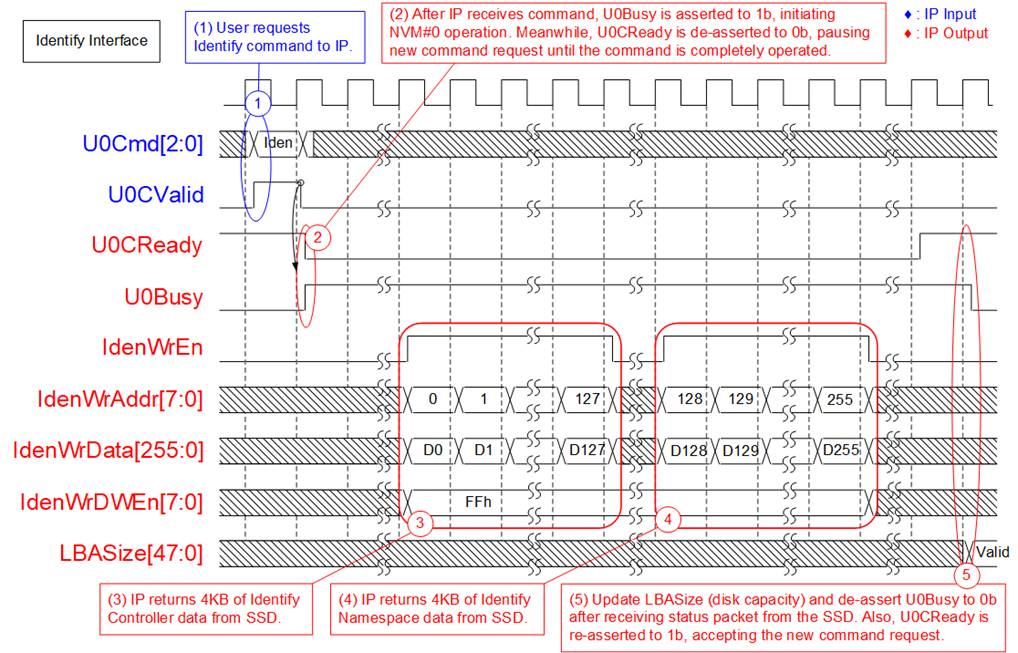
Figure 13 Identify Command Timing Diagram
The execution flow of the Identify command is described below.
1) The user issues an Identify command request to NVM#0 by setting U0Cmd=000b and asserting U0CValid = 1b.
2) Upon receiving the command request, the IP asserts U0Busy to 1b. At the same time, U0CReady is de-asserted to 0b, preventing additional command requests until the current operation is completed.
3) The IP returns 4096-byte Identify Controller data to the user. During this transfer, IdenWrEn is asserted to 1b, and IdenWrAddr ranges from 0 to 63. IdenWrData and IdenWrDWEn are valid when IdenWrEn=1b.
4) The IP then returns 4096-byte Identify Namespace data, with IdenWrAddr ranging from 64 to 127. Bit IdenWrAddr[6] can be used to distinguish between Controller data (0b) and Namespace data (1b).
5) After completing the Identify command, the IP de-asserts U0Busy to 0b and updates LBASize with a valid value. U0CReady is then asserted to 1b, allowing new command requests.
Note: U0CReady is asserted for one clock cycle to acknowledge the command request, followed by U0Busy being de-asserted to 0b to indicate the command completion.
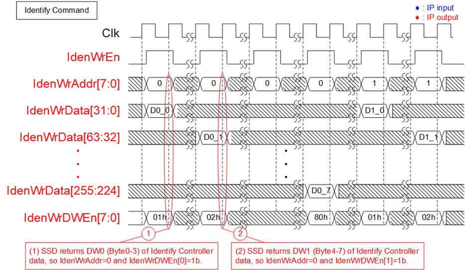
Figure 14 IdenWrDWEn Timing Diagram
The signal IdenWrDWEn is an 8-bit control signal used to validate corresponding segments of a 256-bit data bus that carries 32-bit words. This is used for SSDs that return 4 KB Identify Controller and Identify Namespace data one 32-bit word at a time, rather than as a continuous data stream.
To forward a single 32-bit word during a write cycle, one bit of IdenWrDWEn is asserted to 1b, as illustrated in Figure 14. Each bit of IdenWrDWEn corresponds to a specific 32-bit segment of IdenWrData: bit[0], [1], …, [7] of IdenWrDWEn map to bits[31:0], [63:32], …, [255:224] of IdenWrData, respectively.
Shutdown
The Shutdown command is a command that should be sent as the last command before the system is powered down. The SSD ensures that the data from its internal cache is written to the flash memory before the shutdown process finishes. After the shutdown operation is completed, the rmNVMeG4-IP and the SSD become inactive. If the SSD is powered down without executing the Shutdown command, the total count of unsafe shutdowns is increased, as returned data from the SMART command.
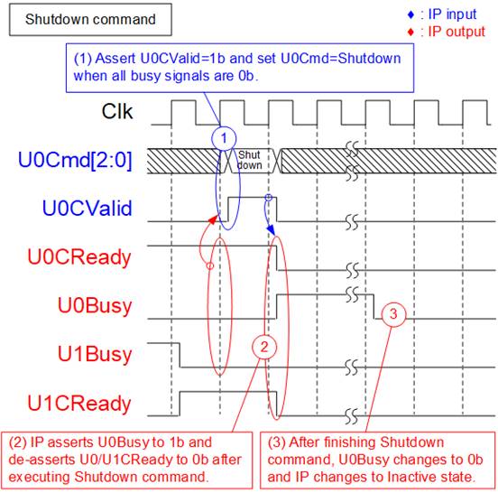
Figure 15 Shutdown Command Timing Diagram
The process for executing the Shutdown command is described below.
1) Before requesting the Shutdown command, both NVM#0 and NVM#1 must be in the Idle state, indicated by U0Busy=0b, U1Busy=0b, and U0CReady=1b. To send Shutdown command, the user asserts U0CValid to 1b and sets U0Cmd=001b.
2) Upon receiving the Shutdown command, the IP asserts U0Busy to 1b, indicating that it is processing the command. Additionally, both U0CReady and U1CReady are de-asserted to 0b, preventing any new command requests.
3) After the completion of the Shutdown command operation, U0Busy is de-asserted to 0b, indicating that the IP is no longer busy. However, U0CReady and U1CReady remain at 0b because the IP does not accept any commands after the Shutdown command.
SMART
The SMART command is the command to check the health of the SSD. When this command is sent, the SSD returns 512-byte health information. The SMART command parameters are loaded from the CtmSubmDW0-DW15 signals on the Custom command interface. The user must set the 16-Dword data which is a constant value before asserting U0CValid. Once the SMART data is returned, it can be accessed via the CtmRAM port, as shown in Figure 16.
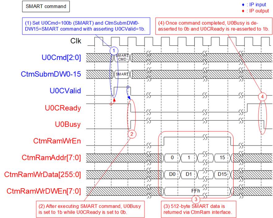
Figure 16 SMART Command Timing Diagram
The execution flow of the SMART command is described below.
1) Ensure that NVM#0 is ready to receive command by checking that U0Busy=0b and U0CReady=1b. The user then asserts U0CValid to 1b with U0Cmd=100b and sets the following values to CtmSubmDW0-DW15 for the SMART command:
CtmSubmDW0 = 0000_0002h
CtmSubmDW1 = FFFF_FFFFh
CtmSubmDW2 – CtmSubmDW5 = 0000_0000h
CtmSubmDW6 = 0802_2000h
CtmSubmDW7 – CtmSubmDW9 = 0000_0000h
CtmSubmDW10 = 007F_0002h
CtmSubmDW11 – CtmSubmDW15 = 0000_0000h
2) NVM#0 acknowledges the SMART command by asserting U0Busy to 1b and de-asserting U0CReady to 0b.
3) The 512-byte SMART data is returned through the CtmRamWrData interface. Valid data is indicated by CtmRamWrEn = 1b. CtmRamAddr indicates the data index (0 to 15) for the 512-byte SMART data. When CtmRamAddr = 0, bytes 0–31 are valid on CtmRamWrData. CtmRamWrDWEn provides DWORD (32-bit) enable for CtmRamWrData. When CtmRamWrDWEn = FFh, all 256 bits of CtmRamWrData are valid.
4) Once the SMART command operation is completed, U0Busy is de-asserted to 0b and U0CReady is asserted to 1b, indicating readiness for the next command.
Note: U0CReady is asserted for one clock cycle to acknowledge the command request, followed by U0Busy being de-asserted to 0b to indicate the command completion.
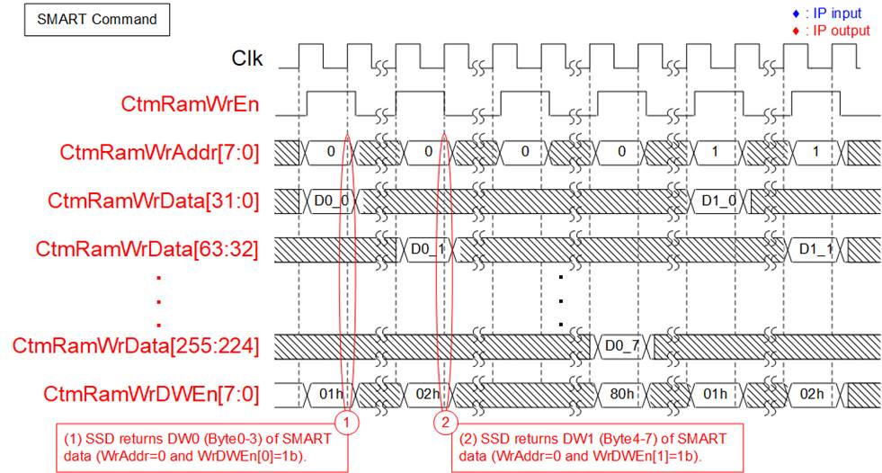
Figure 17 CtmRamWrDWEn Timing Diagram
Similar to Identify command, some SSDs return only one Dword (32-bit) of data at a time instead of streaming 512-byte block continuously. In such cases, one bit of CtmRamWrDWEn is asserted to 1b during the write cycle to indicate that a specific 32-bit segment of CtmRamWrData is valid. Each bit of CtmRamWrDWEn corresponds to a 32-bit segment within the 256-bit CtmRamWrData signal as follows: bit[0], [1], [2], …, and [7] of CtmRamWrDWEn correspond to bits[31:0], [63:32], …, and [255:224] of CtmRamWrData, respectively.
Secure Erase
The Secure Erase is a command that erases all user data in the SSD. After the Secure Erase command is executed, the contents of the user data are indeterminate. Since executing this command may require long time for operation, users need to disable timer of the IP by setting ‘TimeoutSet’ signal to zero value.
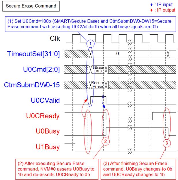
Figure 18 Secure Erase Command Timing Diagram
The execution flow of the Secure Erase command is described below.
1) Ensure that both NVM#0 and NVM#1 are in the Idle state, indicated by U0Busy=0b, U1Busy=0b, and U0CReady=1b. The user issues a Secure Erase command request to NVM#0 by setting U0Cmd=100b and asserting U0CValid = 1b. The TimeoutSet and CtmSubmDW0-DW15 fields must be set to fixed values for the Secure Erase command as follows:
TimeoutSet = 0000_0000h (Disable Timer)
CtmSubmDW0 = 0000_0080h
CtmSubmDW1 = 0000_0001h
CtmSubmDW2 – CtmSubmDW9 = 0000_0000h
CtmSubmDW10 = 0000_0200h
CtmSubmDW11 – CtmSubmDW15 = 0000_0000h
2) Upon receiving the command, NVM#0 asserts U0Busy to 1b and de-asserts U0CReady to 0b.
3) After the Secure Erase operation is completed, U0Busy is de-asserted to 0b and U0CReady is asserted to 1b, indicating readiness for the next command. The TimeOutSet value can then be reconfigured to non-zero value, enabling the timeout function, if required.
Note:
1) U0CReady is asserted for one clock cycle, followed by U0Busy being de-asserted, indicating completion of the operation. The next command can be issued only after U0Busy=0b.
2) Some SSDs may experience a decrease in performance after long data transfer. In such cases, executing the Secure Erase command can help restore the SSD’s performance.
Flush
The SSDs typically enhance write performance by caching write data before writing it to the flash memory. However, unexpected power loss can result in data loss as cached data may not be stored in flash memory. To avoid data loss, the Flush command can be used to force the SSD controller to write cached data to the flash memory.
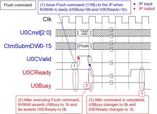
Figure 19 Flush Command Timing Diagram
The execution flow of the Flush command is described below.
1) Ensure that NVM#0 is ready to receive the command by checking that U0Busy=0b and U0CReady=1b. The user then asserts U0CValid to 1b with U0Cmd=110b. For the Flush command, the CtmSubmDW0-DW15 fields must be set to fixed values as follows:
CtmSubmDW0 = 0000_0000h
CtmSubmDW1 = 0000_0001h
CtmSubmDW2 – CtmSubmDW15 = 0000_0000h
2) Upon receiving the Flush command, NVM#0 asserts U0Busy to 1b and de-asserts U0CReady to 0b, indicating that the command is being processed.
3) After the Flush command operation is completed, U0Busy is de-asserted to 0b and U0CReady is asserted to 1b, indicating readiness for the next command.
Executing the Flush command ensures that all data from the previous Write operations is guaranteed to be stored in flash memory, thus preventing data loss in the event of unexpected power loss.
Note: U0CReady is asserted for one clock cycle, followed by U0Busy being de-asserted, indicating completion of the operation. The next command can be issued only after U0Busy=0b.
Error
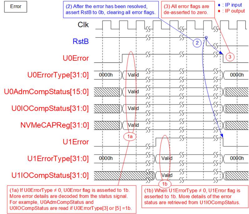
Figure 20 Error Flag Timing Diagram
If an error occurs during initialization or command execution, the U0Error or U1Error flag is asserted to 1b. To identify the error type, the corresponding U0ErrorType or U1ErrorType signal should be examined.
For the User#0 I/F, NVMeCAPReg, U0AdmCompStatus, and U0IOCompStatus provide additional error information after U0Error is asserted. Similarly, for the User#1 I/F, U1IOCompStatus provides detailed error information after U1Error is asserted.
If an error occurs during initialization, it is recommended to check NVMeCAPReg to verify the capabilities of the connected NVMe SSD. If an error occurs during command execution, U0AdmCompStatus or U0/U1IOCompStatus should be examined for further details.
· If bit[3] of U0ErrorType is asserted, refer to the U0AdmCompStatus signal for more detailed error information.
· If bit[5] of U0/U1ErrorType is asserted, refer to the U0/U1IOCompStatus signal for further details.
The U0Error and U1Error flag are cleared only by asserting RstB to 0b. Once the issue is resolved, assert RstB to 0b to reset the IP and clear the error status.
Verification Methods
The rmNVMeG4-IP Core functionality was verified by simulation and also proved on real board design by using ZCU106 evaluation board.
Recommended Design Experience
Experienced design engineers with a knowledge of Vivado Tools should easily integrate this IP into their design.
Ordering Information
This product is available directly from Design Gateway Co., Ltd. Please contact Design Gateway Co., Ltd. for pricing and additional information about this product using the contact information on the front page of this datasheet.
Revision History
|
Revision |
Date (D-M-Y) |
Description |
|
1.00 |
2-Apr-26 |
Initial release |