
Core Facts |
|
|
Provided with Core |
|
|
Documentation |
User Guide, Design Guide |
|
Design File Formats |
Encrypted hdl File |
|
Verification |
A10SoC board @200MHz |
|
Instantiation Templates |
VHDL |
|
Reference Designs & Application Notes |
QuartusII Project, See Demo Instruction |
|
Additional Items |
Arria10 SoC Development Board |
|
Simulation Tool Used |
|
|
- |
|
|
Support |
|
|
Support Provided by Design Gateway Co., Ltd. |
|
Design Gateway Co.,Ltd
E-mail: ip-sales@design-gateway.com
URL: www.design-gateway.com
Features
· Support SHA 256-bit standard function.
· Support input data length up to 261-1 bytes. (264-8 bits)
· Super high throughtput rate at 65 clocks per 64 bytes data (1.015625 cycles/byte).
· Hash speed up to 1.575 Gbps @ 200MHz.
· Simple user interface signals as same as FIFO interface.
Table 1: Example Implementation Statistics for SHA256IP on A10SoC board.
|
Family |
Example Device |
Fmax (MHz) |
ALMs |
LUTs |
Registers(1) |
M20Ks |
Design Tools |
|
Arria10 SX |
10AS066N3F40E2SGE2 |
200 |
761.3 |
1,163 |
1,359 |
1 |
QuartusII 16.0 |
Notes:
(1) Actual logic resource dependent on percentage of unrelated logic.
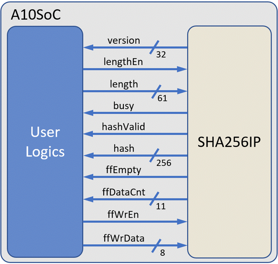
Figure 1: SHA256IP Block Diagram
General Description
SHA256IP implements the SHA-256 algorithm which is widely used for authenticating in many applications. Such as communication, password authentication, and also data authentication in blockchain system.
Functional Description
Table 1 shows interface signals of SHA256IP.
Table 1 I/O signals
|
Signal name |
Dir |
Description |
|
rstB |
In |
IP core system reset. Active low. |
|
clk |
In |
IP core system clock. |
|
version[31:0] |
Out |
32-bit version number of SHA256IP |
|
HASH function control signals |
||
|
lengthEn |
In |
lengthEn is signal to set length of data for hash function. And SHA256IP will start to wait data. |
|
length[60:0] |
In |
data length in byte unit. |
|
busy |
Out |
busy is actived after user set lengthEn, until SHA256IP get all data and finish hash process. |
|
hashValid |
Out |
hashValid signal is actived 1 cycle at the end of hash process, user can capture hash result at this cycle. |
|
hash[255:0] |
Out |
256-bit hash result |
|
Input data interface (FIFO interface) |
||
|
ffWrEn |
In |
ffWrEn is control signal to write ffWrData[7:0] to internal memory. |
|
ffWrData[7:0] |
In |
8-bit input data. |
|
ffEmpty |
Out |
ffEmpty
is empty status of internal memory to wait for input data. |
|
ffDataCnt[10:0] |
Out |
ffDataCnt[10:0]
is current valid data in byte unit. User must pause data transfer when
remained buffer is less than 64 bytes (ffDataCnt[10:0] > x"7C0") |
SHA256IP operation is as simple as 3 steps as below and Figure 2 shows timing diagram of SHA256IP interface signals.
· Set length of data
The hash operation is started after user set lengthEn = ‘1’ and data size is set in length[60:0] signal on the same cycles.
The busy signal is actived to be ‘1’ until SHA256IP get all data and finished hash function.
· Input data transfer
After set length to SHA256IP, SHA256IP wait for data with same size of length. The hash function is calculated while data is transferring.
Data interface signals is as simple as 8-bit FIFO interface signals. User logic must pause data transfer when ffDataCnt[[10:0] is existed “7C0” value because SHA256IP need interface data buffer at least 64 bytes.
· Hash result valid
After SHA256IP receive all data equal with specific length and hash function is finished, hash value is set to hash[255:0] signal while hashValid signal is set to be ‘1’. Then busy is set to be ‘0’ in next cycle, and wait for next operation cycle.
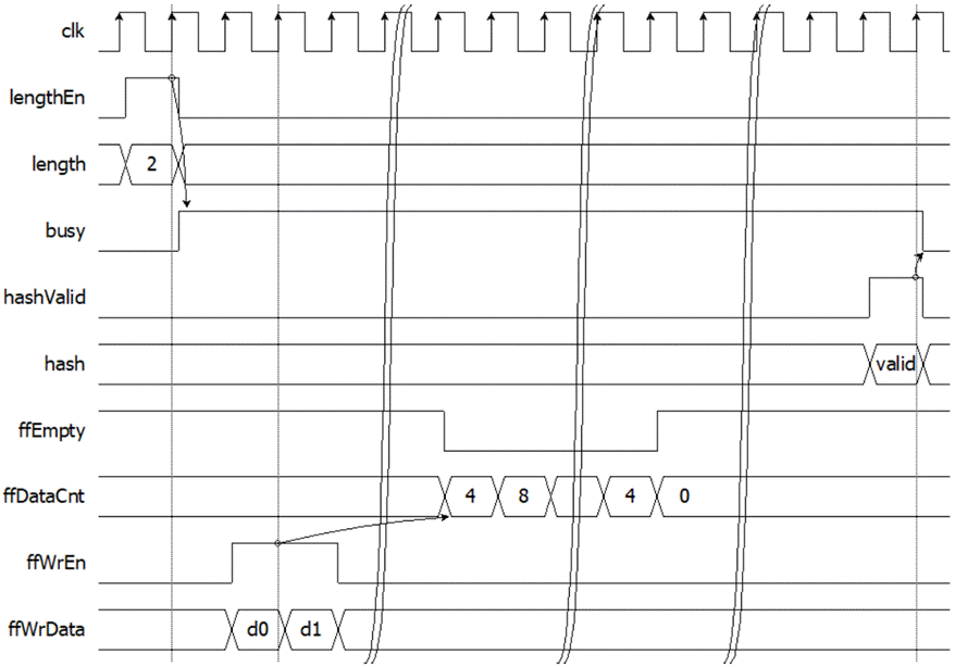
Figure 2: SHA256IP interface timing diagram
Verification Methods
The SHA256IP Core functionality was verified on real board design by using Arria10 SoC development board.
Recommended Design Experience
User must be familiar with HDL design methodology to integrate this IP into system.
Ordering Information
This product is available directly from Design Gateway Co., Ltd. Please contact Design Gatway Co., Ltd. For pricing and additional information about this product using the contact information on the front page of this datasheet.
Revision History
|
Revision |
Date |
Description |
|
1.00 |
26/Jan/2021 |
New release |