TOE100G-IP with CPU Reference Design
Rev2.1 30-May-23
3.6 Function list in User application
4.1 “tcpdatatest” for half duplex test
4.2 “tcp_client_txrx_xg” for full duplex test
1 Introduction
The TCP/IP is the Internet Protocol Suite for networking applications, consisting of four layers: Application, Transport, Internet, and Network Access. Figure 1‑1 shows how the Network Access layer is split into two sublayers, Link and Physical, to link them with the hardware implementation using an FPGA.
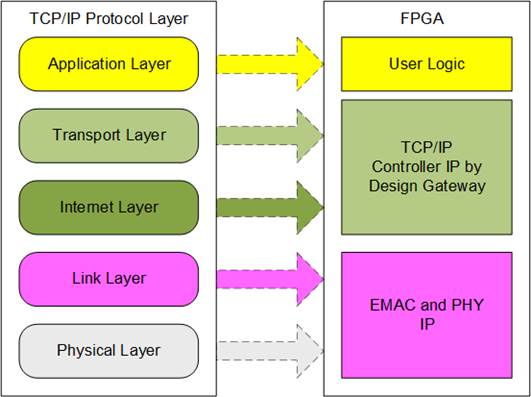
Figure 1‑1 TCP/IP protocol layer
The Link and Physical layers are typically implemented using Intel IP cores, which provide the IP suite with Ethernet MAC, PCS, and PMA features. The IP name is different in each FPGA model such as Low Latency 100G Ethernet Intel FPGA IP for Stratix 10 device.
The TOE100G-IP implements the Transport and Internet layer of TCP/IP Protocol using full hardwire logic, without the need for a CPU or DDR. This allows the user logic to be designed for processing the TCP payload data at the user interface of TOE100G-IP. The TOE100G-IP is responsible for building an Ethernet packet that contains the TCP payload data form the user and transmitting it to the Ethernet MAC (EMAC). If the user data size is too large to fit in one Ethernet packet, the TOE100G-IP will split the data into multiple packets to send it. To construct a complete Ethernet packet, the TOE100G-IP must process and append the TCP/IP header to the packet before transmitting. On the other hand, when the TOE100G-IP receives an Ethernet packet from EMAC, it extracts and verifies the packet. If the packet is valid, the TOE100G-IP extracts TCP payload data from the packet and forwards it to the user logic. Otherwise, the packet is rejected.
The reference design includes a simple user logic, TOE100G-IP, and 100G Ethernet for data transfer using TCP/IP protocol. The data can be transferred with the target, which may be a PC or another FPGA with integrating TOE100G-IP. Design Gateway provides two test applications on the PC for testing the demo using one TCP session, “tcpdatatest” for half-duplex (send or receive data test) and “tcp_client_txrx_xg” for full-duplex (send and receive data simultaneously) using one TCP session.
To provide flexibility in testing, the user can set test parameters and control the operation of the TOE100G-IP demo via JTAG UART, which is integrated with a CPU system. The user can monitor the current status and set test parameters through the console. The CPU firmware is built using a simple bare-metal OS. More details of the demo are described below.
2 Hardware overview
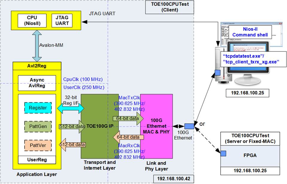
Figure 2‑1 Demo block diagram
In the test environment, two devices are used to transfer data over a 100G Ethernet connection. The first device is an FPGA which is initialized in Client mode, and the second device can be a PC or another FPGA which is initialized in Server mode. When using two FPGAs, there are additional initialization options available, i.e., Client <–> Fixed-MAC or Fixed-MAC <-> Fixed-MAC. Two test applications (tcpdatatest and tcp_client_txrx_xg) are provided for transferring data between the PC and FPGA.
In the FPGA system, the TOE100G-IP is connected to the 100G Ethernet MAC and PHY to implement all TCP/IP layers. The user interface of the TOE100G-IP is connected to UserReg within Avl2Reg, which includes a Register file for interfacing with the Register interface, PattGen for sending test data via Tx FIFO interface, and PattVer for verifying test data via Rx FIFO interface. The Register file of UserReg is controlled by CPU firmware through the Avalon-MM bus.
The test design uses four clock domains: CpuClk for the CPU system, MacTxClk and MacRxClk for the Tx and Rx user interface of EMAC IP, and UserClk which for the user logic of the TOE100G-IP. Therefore, AsyncAvlReg is designed to support asynchronous signal transferring between CpuClk and UserClk. More information about each module inside the TOE100CPUTest is described below.
Note:
1. UserClk can be modified to use the same clock as CpuClk to reduce clock resource.
2. The UserClk frequency of TOE100G-IP is recommended to be 220 MHz or higher.
3. The MacTxClk and MacRxClk of the 100G Ethernet Soft IP, such as Low Latency 100G Ethernet Intel FPGA IP on Stratix 10 device, are separate clocks, but they have the same frequencies of 390.625 MHz. On the other hand, the MacTxClk and MacRxClk of the 100G Ethernet Hard IP, such as E-tile Hard IP on Agilex 7 device, are the same clock signals, with a frequency of 402.832 MHz.
2.1 100G Ethernet MAC and PHY
The 100G Ethernet MAC and PHY comprises the MAC, PCS, and PMA layers for interfacing with external devices using 100G BASE-SR. This section describes two solutions on two FPGA models in more detail.
1) Low Latency 100G Ethernet Intel FPGA IP on Stratix 10 devices
This is the soft IP core and its user interface is a 512-bit Avalon-stream at 390.625 MHz, which can be directly connected to TOE100G-IP. However, the Tx user interface and Rx user interface are run in the different clock domains. For more information, visit the Intel website and check out the “Low Latency 100G Ethernet Intel FPGA IP Core User Guide: For Intel Stratix10 Devices”.
https://www.intel.com/content/www/us/en/docs/programmable/683100/21-1-19-2-0/ip-overview.html
2) E-tile Hard IP for Ethernet on Agilex 7 devices.
This is the hard IP core and its user interface is a 512-bit Avalon-stream at 402.832 MHz, which can be directly connected to TOE100G-IP. The Tx and Rx user interface is run in the same clock domains. For more information, visit the Intel website and check out the “E-Tile Hard IP User Guide”.
Note: The default reference design enables the RS-FEC feature on the 100G Ethernet (MAC) Subsystem. So, please ensure that the network equipment in the test environment supports RS-FEC feature. Contact us for the demo system that disables RS-FEC feature.
2.2 TOE100G-IP
TOE100G-IP implements TCP/IP stack and fully offload engine without requiring the CPU and the external memory. User interface has two signal groups - control signals and data signals. Control and status signals use Single-port RAM interface for write/read register access. Data signals use FIFO interface for transferring data stream in both directions. The interface with 100G Ethernet MAC is a 512-bit Avalon-stream interface. More information can be found from the datasheet.
https://dgway.com/products/IP/TOE100G-IP/dg_toe100gip_data_sheet_intel.pdf
2.3 CPU and Peripherals
The CPU system uses a 32-bit Avalon-MM bus as the interface to access peripherals such as the Timer and JTAG UART. The system also integrates an additional peripheral to access the test logic by assigning a unique base address and address range. To support CPU read and write operations, the hardware logic must comply with the Avalon-MM bus standard. Avl2Reg module, as shown in Figure 2‑2, is designed to connect the CPU system via the Avalon-MM interface, in compliance with the standard.
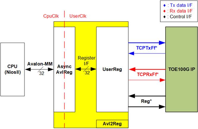
Figure 2‑2 Avl2Reg block diagram
Avl2Reg consists of AsyncAvlReg and UserReg. AsyncAvlReg converts Avalon-MM signals into a Register interface with a 32-bit data bus size, similar to Avalon-MM data bus size. It also includes asynchronous logic to handle clock domain crossing between the CpuClk and UserClk domains.
UserReg includes the Register file of the parameters and the status signals of test logics. Both the data interface and control interface of TOE100G-IP are connected to UserReg. Further details of AsyncAvlReg and UserReg are described below.
2.3.1 AsyncAvlReg
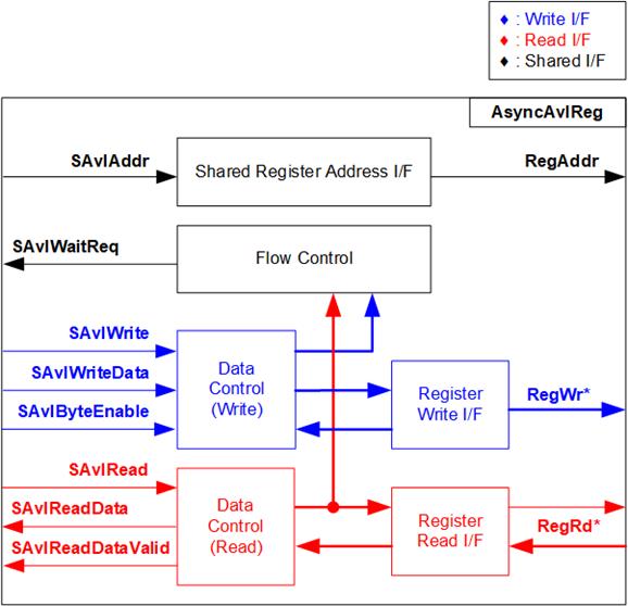
Figure 2‑3 AsyncAvlReg interface
The Avalon-MM bus interface signal can be grouped into three categories: Write channel (blue), Read channel (red), and Shared control channel (black). More details about the Avalon-MM interface specification can be found in the following document.
https://www.intel.com/content/dam/www/programmable/us/en/pdfs/literature/manual/mnl_avalon_spec.pdf
According to Avalon-MM specification, only one command (write or read) can be executed at a time. AsyncAvlReg’s logic is divided into three groups: Write control logic, Read control logic, and Flow control logic. The flow control logic asserts SAvlWaitReq to hold the next request from the Avalon-MM interface if the current request has not finished. Write control and Write data I/F of the Avalon-MM bus are latched and transferred to the Write register interface with clock domain crossing registers. Similarly, Read control I/F are latched and transferred to be Read register interface. Afterward, the data returned from Register Read I/F is transferred to Avalon-MM bus with using clock domain crossing registers. The Address I/F of Avalon-MM is also latched and transferred to the Address register interface.
The Register interface is compatible with the single-port RAM interface for write transactions. However, the read transaction of the Register interface is slightly modified from RAM interface by adding RdReq and RdValid signals to control the read latency time. Since the address of the Register interface is shared for write and read transactions, the user cannot write and read the register at the same time. The timing diagram of the Register interface is shown in Figure 2‑4.
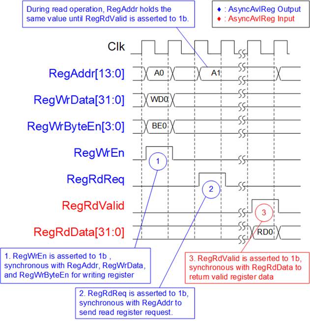
Figure 2‑4 Register interface timing diagram
1) Timing diagram to write register is similar to that of a single-port RAM. The RegWrEn signal is set to 1b, along with a valid RegAddr (Register address in 32-bit units), RegWrData (write data for the register), and RegWrByteEn (write byte enable). The byte enable consists of four bits that indicate the validity of the byte data. For example, bit[0], [1], [2], and [3] are set to 1b when RegWrData[7:0], [15:8], [23:16], and [31:24] are valid, respectively.
2) To read register, AsyncAvlReg sets the RegRdReq signal to 1b with a valid value for RegAddr. The 32-bit data is returned after the read request is received. The slave detects the RegRdReq signal being set to start the read transaction. In the read operation, the address value (RegAddr) remains unchanged until RegRdValid is set to 1b. The address can then be used to select the returned data using multiple layers of multiplexers.
3) The slave returns the read data on RegRdData bus by setting the RegRdValid signal to 1b. After that, AsyncAvlReg forwards the read value to the SAvlRead interface.
2.3.2 UserReg
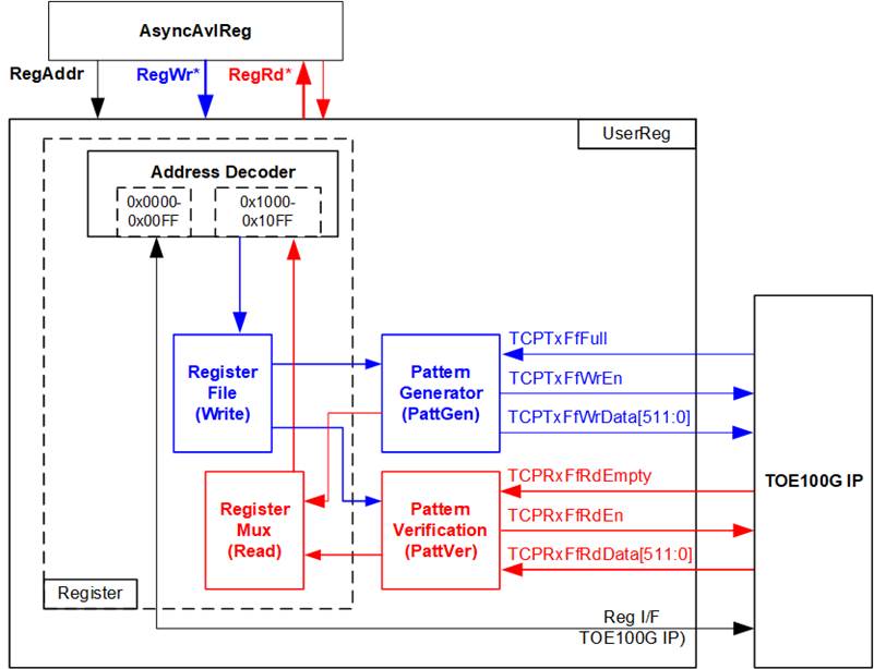
Figure 2‑5 UserReg block diagram
The UserReg module includes three functions: Register, Pattern generator (PattGen), and Pattern verification (PattVer). The Register block decodes the requested address from AsyncAvlReg and selects the active register for a write or read transaction. The PattGen block is designed to send 512-bit test data to TOE100G-IP following FIFO interface standard, while the PattVer block is designed to read and verify 512-bit data from TOE100G-IP following FIFO interface standard.
Register Block
The address range, mapped to UserReg, is split into two areas: TOE100G-IP register (0x0000-0x00FF) and UserReg register (0x1000-0x10FF). The Address decoder decodes the upper bits of RegAddr to select the active hardware. Since the Register file inside UserReg is 32-bit bus size, Write byte enable (RegWrByteEn) is not used. To write hardware registers, the CPU must use a 32-bit pointer to place a 32-bit valid value on the write data bus.
For reading a register, a multiplexer selects the data to return to CPU by using the address. The lower bits of RegAddr are applied to select the active data within each Register area. While the upper bits are used to select the returned data from each Register area. The total latency time of read data is equal to one clock cycle, and RegRdValid is created by RegRdReq by asserting a D Flip-flop. More details of the address mapping within the UserReg module are shown in Table 2‑1.
Table 2‑1 Register map Definition
|
Register Name |
Description |
|
|
Wr/Rd |
(Label in the “toe100gtest.c”) |
|
|
BA+0x0000 – BA+0x00FF: TOE100G-IP Register Area More details of each register are described in TOE100G-IP datasheet. |
||
|
BA+0x0000 |
TOE_RST_INTREG |
Mapped to RST register within TOE100G-IP |
|
BA+0x0004 |
TOE_CMD_INTREG |
Mapped to CMD register within TOE100G-IP |
|
BA+0x0008 |
TOE_SML_INTREG |
Mapped to SML register within TOE100G-IP |
|
BA+0x000C |
TOE_SMH_INTREG |
Mapped to SMH register within TOE100G-IP |
|
BA+0x0010 |
TOE_DIP_INTREG |
Mapped to DIP register within TOE100G-IP |
|
BA+0x0014 |
TOE_SIP_INTREG |
Mapped to SIP register within TOE100G-IP |
|
BA+0x0018 |
TOE_DPN_INTREG |
Mapped to DPN register within TOE100G-IP |
|
BA+0x001C |
TOE_SPN_INTREG |
Mapped to SPN register within TOE100G-IP |
|
BA+0x0020 |
TOE_TDL_INTREG |
Mapped to TDL register within TOE100G-IP |
|
BA+0x0024 |
TOE_TMO_INTREG |
Mapped to TMO register within TOE100G-IP |
|
BA+0x0028 |
TOE_PKL_INTREG |
Mapped to PKL register within TOE100G-IP |
|
BA+0x002C |
TOE_PSH_INTREG |
Mapped to PSH register within TOE100G-IP |
|
BA+0x0030 |
TOE_WIN_INTREG |
Mapped to WIN register within TOE100G-IP |
|
BA+0x0034 |
TOE_ETL_INTREG |
Mapped to ETL register within TOE100G-IP |
|
BA+0x0038 |
TOE_SRV_INTREG |
Mapped to SRV register within TOE100G-IP |
|
BA+0x003C |
TOE_VER_INTREG |
Mapped to VER register within TOE100G-IP |
|
BA+0x0040 |
TOE_DML_INTREG |
Mapped to DML register within TOE100G-IP |
|
BA+0x0044 |
TOE_DMH_INTREG |
Mapped to DMH register within TOE100G-IP |
|
BA+0x1000 – BA+0x10FF: UserReg control/status |
||
|
BA+0x1000 |
Total transmit length |
Wr [31:0] – Total amount of transmitted data in 512-bit unit. Valid from 1-0xFFFFFFFF. Rd [31:0] – Current amount of transmitted data in 512-bit unit. The value is cleared to 0 when USER_CMD_INTREG is written by user. |
|
Wr/Rd |
(USER_TXLEN_INTREG) |
|
|
BA+0x1004 |
User Command |
Wr [0] – Start transmitting. Set 0b to start transmitting. [1] – Data verification enable (0b: Disable data verification, 1b: Enable data verification) Rd [0] – Busy of PattGen inside UserReg (0b: Idle, 1b: PattGen is busy) [1] – Data verification error (0b: Normal, 1b: Error) This bit is auto-cleared when user starts new operation or reset. [2] – Mapped to ConnOn signal of TOE100G-IP |
|
Wr/Rd |
(USER_CMD_INTREG) |
|
|
BA+0x1008 |
User Reset |
Wr 0] – Reset signal. Set 1b to reset UserReg. This bit is auto-cleared to 0b. [8] – Set 1b to clear TimerInt latched value Rd [8] – Latched value of TimerInt, the output from IP (0b: Normal, 1b: TimerInt=1b has been asserted) This flag can be cleared by system reset condition or setting USER_RST_INTREG[8]=1b. [16] – Ethernet linkup status from Ethernet MAC (0b: Link down, 1b: Link up) |
|
Wr/Rd |
(USER_RST_INTREG) |
|
|
Address |
Register Name |
Description |
|
Wr/Rd |
(Label in the “toe100gtest.c”) |
|
|
BA+0x1000 – BA+0x10FF: UserReg control/status |
||
|
BA+0x100C |
FIFO status |
Rd[5:0] - Mapped to TCPRxFfLastRdCnt signal of TOE100G-IP [19:6] - Mapped to TCPRxFfRdCnt signal of TOE100G-IP [24] - Mapped to TCPTxFfFull signal of TOE100G-IP |
|
Rd |
(USER_FFSTS_INTREG) |
|
|
BA+0x1010 |
Total receive length |
Rd[31:0] – Current amount of received data from TOE100G-IP in 512-bit unit. The value is cleared to 0 when USER_CMD_INTREG is written by user. |
|
Rd |
(USER_RXLEN_INTREG) |
|
|
BA+0x1020 |
Connection interrupt |
Wr[0] – Set 1b to clear the Connection interrupt (USER_INT_INTREG[0]) Rd[0] – Interrupt when ConnOn edge has been detected (1b: Detect edge of ConnOn signal from TOE100G-IP, 0b: ConnOn does not change the value.) Note: ConnOn value can be read from USER_CMD_INTREG[2]. |
|
Wr/Rd |
(USER_INT_INTREG) |
|
|
BA+0x1080 |
EMAC IP version |
Rd[31:0] – Mapped to IPVersion output from DG EMAC-IP when the system integrates DG EMAC-IP. In this demo, it is equal to 0. |
|
Rd |
(EMAC_VER_INTREG) |
|
Pattern Generator
The logic diagram and timing diagram of Pattern Generator (PattGen) are illustrated in Figure 2‑6 and Figure 2‑7, respectively.
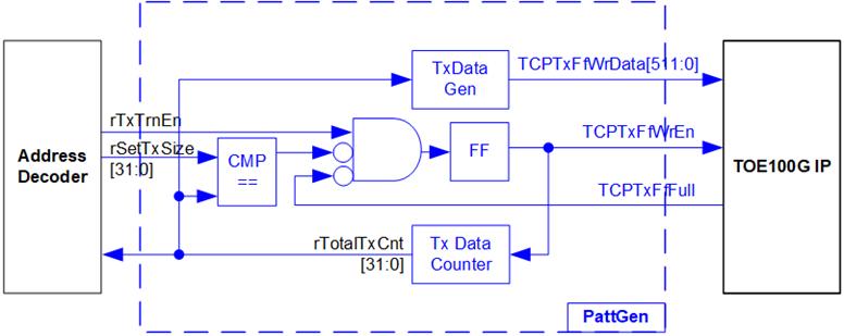
Figure 2‑6 PattGen block
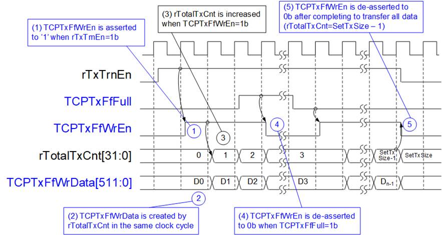
Figure 2‑7 PattGen timing diagram
When USER_CMD_INTREG[0] is set to 0b, PattGen initiates the operation of generating test data by setting rTxTrnEn to 1b. While rTxTrnEn remains set to 1b, TCPTxFfWrEn is controlled by TCPTxFfFull. If TCPTxFfFull is 1b, TCPTxFfWrEn is de-asserted to 0b. The data counter, rTotalTxCnt, checks the total amount of data sent to TOE100G-IP. The lower bits of rTotalTxCnt generate 32-bit incremental data for the TOETxFfWrData signal. Once all data has been transferred, equal to rSetTxSize, rTxTrnEn is de-asserted to 0b.
Pattern Verification
The logic diagram and timing diagram of Pattern Verification (PattVer) are illustrated in Figure 2‑8 and Figure 2‑9, respectively. The verification feature is executed when the verification flag (rVerifyEn) is enabled.
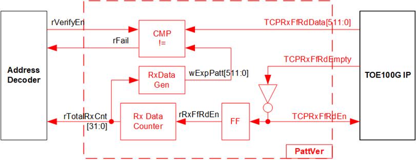
Figure 2‑8 PattVer block
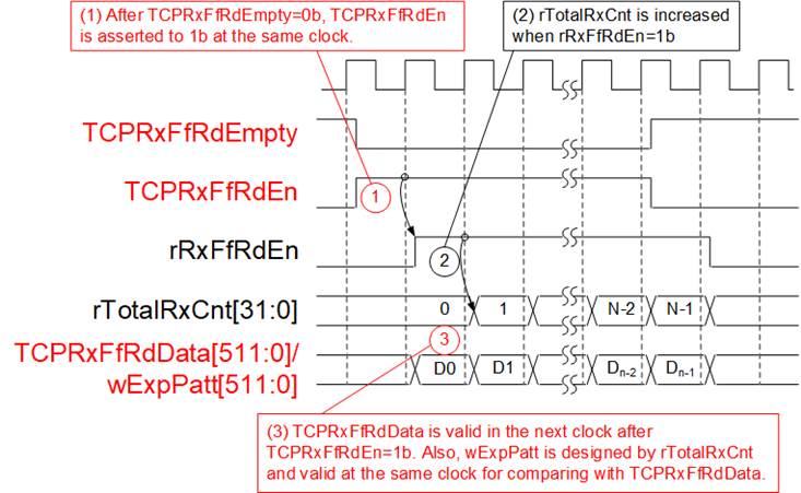
Figure 2‑9 PattVer Timing diagram
When rVerifyEn is set to 1b, the verification logic is processed. It compares the received data (TCPRxFfRdData) with the expected data (wExpPatt). If comparison fails, rRdFail is asserted to 1b. The TCPRxFfRdEn signal is created by applying NOT logic to TCPRxFfRdEmpty. The data for comparison, TCPRxFfRdData, becomes valid in the next clock cycle. To count the total size of received data, rTotalRxCnt is enabled by rRxFfRdEn, which is delayed by one clock cycle from TCPRxFfRdEn. rTotalRxCnt are applied to generate wExpPatt for comparison with TCPRxFfRdData. Therefore, TCPRxFfRdData and wExpPatt are valid in the same clock cycle and can be compared using rRxFfRdEn signal.
3 CPU Firmware on FPGA
The reference design uses a bare-metal OS for the CPU firmware operating, which facilitates hardware handling. When executing the test system, the first step is to initialize the hardware, described in more details below.
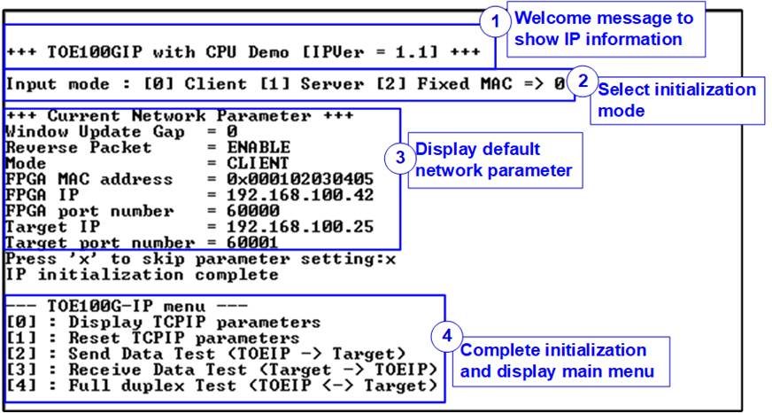
Figure 3‑1 System initialization in Client mode by using default parameters
Figure 3‑1 illustrates the four-step process for hardware initialization, which is described below.
1) Upon FPGA boot-up, the firmware polls the status of the 100G Ethernet link (USER_RST_INTREG[16]). The CPU waits until the link is up, and then displays a welcome message to show IP information.
2) The menu to select the initialization mode of TOE100G-IP is displayed, allowing the user to choose the Client, Server, or Fixed-MAC mode.
Note:
- When running in Client mode, TOE100G-IP sends an ARP request to obtain the MAC address of the target device from the ARP reply. When running in Server mode, TOE100G-IP waits until an ARP request is received to decode the MAC address and return an ARP reply. When running in Fixed-MAC mode, the user needs to know MAC address of the target device for setting to TOE100G-IP.
- When running the test environment with an FPGA board and a PC, it is recommended to set the FPGA to run as Client mode.
- When using two FPGA boards in a test environment, there are three options to establish the connection between them. The first option is to set one board as the Client and the other as the Server. The second option is to configure both boards in Fixed-MAC mode. The third option is to set one board to Fixed-MAC mode and the other board to act as the Client.
3) The CPU displays the default values of the network parameters including Window update gap value, Reverse packet enable flag, the initialization mode, FPGA MAC address, FPGA IP address, FPGA port number, Target IP address, and Target port number. The firmware has two default parameter sets for the operation mode: Server parameter set (used for Server mode only) and Client parameter set (used for both Client and Fixed-MAC mode). When setting to Fixed-MAC mode, an extra parameter, Target MAC address, is also displayed. The user can select to complete the initialization process using the default parameters or by updating some parameters. The details of how to change the parameter are provided in Reset parameters menu (topic 3.2).
4) The CPU waits until the IP completes the initialization process by checking if busy status (TOE_CMD_INTREG[0]) is equal to 0b. After that, “IP initialization complete” is displayed with the main menu. There are five test operations in the main menu, and more details of each menu are described below.
3.1 Display parameters
This menu displays the current value of all TOE100G-IP parameters. The following steps are executed to display parameters.
1) Read the initialization mode.
2) Read all network parameters from each variable in the firmware following the initialization mode, i.e., Window update threshold, Reverse packet enable, source (FPGA) MAC address, source (FPGA) IP address, source (FPGA) port number, Target MAC address (only displayed in fixed MAC mode), Target IP address, and Target port number.
Note: The source parameters are the FPGA parameters set to TOE100G-IP, while the Target parameters are the parameters of a PC or another FPGA.
3) Print out each variable.
3.2 Reset parameters
This menu is used to change some TOE100G-IP parameters, such as IP address and source port number. After setting the updated values to TOE100G-IP registers, the CPU resets to re-initialize the IP using new parameters. Finally, the CPU waits until the initialization is completed, monitored by busy flag. The following steps are executed to reset the parameters.
1) Display all parameters on the console, similar to topic 3.1 (Display parameters).
2) If the user uses the default value, skip to the next step. Otherwise, display the menu to set all parameters.
i) Receive initialization mode from the user. If the initialization is changed, display the latest parameter set of new mode on the console.
ii) Receive the remaining parameters from the user and validate each input separately. If an input is found to be invalid, that particular parameter will not be updated.
3) Force reset to PattGen and PattVer logic by setting USER_RST_INTREG[0]=1b.
4) Force reset to TOE100G-IP by setting TOE_RST_INTREG[0]=1b.
5) Set all parameters to TOE100G-IP registers, such as TOE_SML_INTREG and TOE_DIP_INTREG.
6) De-assert TOE100G-IP reset by setting TOE_RST_INTREG[0]=0b to initiate the initialization process of TOE100G-IP.
7) Monitor the TOE100G-IP busy flag (TOE_CMD_INTREG[0]) until the initialization process is completed (busy flag is de-asserted to 0b).
3.3 Send data test
This test process consists of three user inputs to set total transmit length, packet size, and connection mode (active open for Client connection mode or passive open for Server connection mode). If any of the inputs are invalid, the operation is cancelled. During the test, 32-bit incremental data is generated from the logic and sent to either PC or FPGA. The data is then verified by the test application on PC or by the verification module in FPGA. The operation is considered complete when all the data are transferred from FPGA to PC/FPGA. The sequence of the test is as follows.
1) Receive transfer size, packet size, and connection mode from user and verify if all inputs are valid.
2) Set UserReg registers, including transfer size (USER_TXLEN_INTREG), reset flag to clear initial value of the test pattern (USER_RST_INTREG[0]=1b), and command register to start data pattern generator (USER_CMD_INTREG=0). After that, test pattern generator in UserReg starts sending data to TOE100G-IP.
3) Display recommended parameters of test application on PC by reading the current system parameters.
4) Open connection following connection mode setting.
i) For active open, CPU sets TOE_CMD_INTREG=2 (Open port). After that, it waits until the Connection interrupt status (USER_INT_INTREG[0]) is equal to 1b. If the busy flag of TOE100G-IP (TOE_CMD_INTREG[0]) is de-asserted to 0b but the interrupt is not asserted, the error message is displayed, and it returns to the main menu.
ii) For passive open, CPU waits until the connection is opened by another device (PC or FPGA). Connection interrupt status (USER_INT_INTREG[0]) is monitored until it is equal to 1b.
5) Set the packet size to the TOE100G-IP register (TOE_PKL_INTREG) and calculate the total number of loops from the total transfer size. The maximum transfer size of each loop is 4 GB. The operation of each loop is as follows.
i) Set the transfer size of this loop to TOE100G-IP register (TOE_TDL_INTREG). The transfer size is fixed to 4 GB except the last loop which is equal to the remaining size.
ii) Set the send command to TOE100G-IP register (TOE_CMD_INTREG=0).
iii) Wait until operation is completed by monitoring busy flag (TOE_CMD_INTREG[0]=0b). While monitoring the busy flag, the CPU reads the current amount of transmitted data from user logic (USER_TXLEN_INTREG) and displays the results on the console every second.
6) Set the close connection command to the TOE100G-IP register (TOE_CMD_INTREG=3). Similar to active open, the operation is successful when Connection interrupt status (USER_INT_INTREG[0]) is asserted to 1b. Otherwise, the error message is displayed if TOE100G-IP busy flag (TOE_CMD_INTREG[0]) is de-asserted without the asserting of Connection interrupt status.
7) Calculate performance and show test result on the console.
3.4 Receive data test
The user specifies the total amount of data to be received, the data verification mode (enabled or disabled), and the connection mode (active open for Client connection mode or passive open for Server connection mode). If any of the inputs are invalid, the operation is cancelled. During the test, 32-bit incremental data is generated to verify the received data from either PC or FPGA when data verification mode is enabled. The sequence of this test is as follows.
1) Receive the total transfer size, data verification mode, and connection mode from the user input. Verify that all inputs are valid.
2) Set the UserReg registers.
i) Reset flag to clear the initial value of test pattern (USER_RST_INTREG[0]=1b)
ii) Data verification mode (USER_CMD_INTREG[1]=0b to only read the received data or 1b to read and verify the received data).
3) Display the recommended parameter (similar to Step 3 of Send data test).
4) Open the connection following the connection mode (similar to Step 4 of Send data test).
5) Wait until the connection is closed by the other device (PC or FPGA). ConnOn status (USER_CMD_INTREG[2]) is monitored until it is equal to 0b. While monitoring Connon, the CPU reads the current amount of received data from the user logic (USER_RXLEN_INTREG) and displays the results on the console every second.
Note: USER_FFSTS_INTREG[19:6] is mapped from the TCPRxFfRdCnt signal of TOE100G-IP, which represents the number of data in the FIFO that can be read in 512-bit unit. Therefore, the amount of data that cannot yet be read from the FIFO, indicated by USER_FFSTS_INTREG[5:0] (or TCPRxFfLastRdCnt), should be neglected.
7) Compare the received length of user logic (USER_RXLEN_INTREG) with the set value from the user. If all data is completely received, the CPU checks verification result by reading USER_CMD_INTREG[1] (0b: normal, 1b: error). If some errors are detected, the error message is displayed.
8) Calculate performance and show the test result on the console.
3.5 Full duplex test
This menu enables full duplex testing by simultaneously transferring data between the FPGA and another device (PC/FPGA) in both directions using the same port number. The user provides four inputs: total data size for both transfer directions, packet size for FPGA sending logic, data verification mode for FPGA receiving logic, and connection mode (active open/close for client operation or passive open/close for server operation).
When running the test with a PC, the transfer size set on the FPGA must match the size set on the test application (tcp_client_txrx_xg). The connection mode on the FPGA must be set to passive (server operation) when running with a PC.
The test runs in a forever loop until the user cancels the operation by entering any keys on the FPGA console and then entering Ctrl+C on the PC console. The test sequence is as follows.
1) Receive the total data size, packet size, data verification mode, and connection mode from the user and verify that all inputs are valid.
2) Display the recommended parameters of the test application that runs on the PC from the current system parameters.
3) Set UserReg registers, including the transfer size (USER_TXLEN_INTREG), reset flag to clear the initial value of the test pattern (USER_RST_INTREG[0]=1b), and command register to start the data pattern generator with data verification mode
(USER_CMD_INTREG=1 or 3).
4) Open the connection following the connection mode (similar to Step 4 of Send data test).
5) Set the packet size to TOE100G-IP registers (TOE_PKL_INTREG=user input) and calculate total transfer size in each loop. The maximum size of each loop is 4 GB. The operation of each loop is as follows.
i) Set the transfer size of this loop to TOE_TDL_INTREG. The transfer size is fixed to maximum size (4GB) which is also aligned to the packet size, except the last loop. The transfer size of the last loop is equal to the remaining size.
ii) Set the send command to the TOE100G-IP register (TOE_CMD_INTREG=0).
iii) Wait until the send command is completed by monitoring the busy flag (TOE_CMD_INTREG[0] =0b). While monitoring the busy flag, the CPU reads the current amount of transmitted data and received data from the user logic (USER_TXLEN_INTREG and USER_RXLEN_INTREG) and displays the results on the console every second.
6) Close the connection following the connection mode value.
a) For active close, the CPU waits until the total amount of received data is equal to the set value from the user. Then, set USER_CMD_INTREG=3 to close the connection. Next, the CPU waits until the Connection interrupt status (USER_INT_INTREG[0]]) is asserted to 1b. Otherwise, an error message is displayed if the TOE100G-IP busy flag (TOE_CMD_INTREG[0]) is de-asserted without the asserting of the Connection interrupt status.
b) For passive close, the CPU waits until the connection is closed by the other device (PC or FPGA). The Connection interrupt status (USER_INT_INTREG[0]) is monitored until it is equal to 1b.
7) Check the result and any error (similar to Step 6-7 of Receive data test).
8) Calculate the performance and show the test result on the console. Go back to step 3 to repeat the test in a forever loop.
3.6 Function list in User application
This topic describes the function list to run TOE100G-IP operation.
|
int exec_port(unsigned int port_ctl, unsigned int mode_active) |
|
|
Parameters |
port_ctl: 1-Open port, 0-Close port mode_active: 1-Active open/close, 0-Passive open/close |
|
Return value |
0: The open/close connection is successful -1: Fail to open/close the connection |
|
Description |
To initiate an active mode connection, set the TOE_CMD_INTREG register to either open or close the connection based on the port_ctl mode. Then, monitor the bit0 of USER_INT_INTREG register, which indicates the connection status interrupt, until it is asserted. Once the interrupt flag is set, it will be cleared. |
|
void init_param(void) |
|
|
Parameters |
None |
|
Return value |
None |
|
Description |
Reset parameter following the description in topic 3.2. In the function, show_param and input_param function are called to display parameters and get parameters from user. |
|
int input_param(void) |
|
|
Parameters |
None |
|
Return value |
0: Valid input, -1: Invalid input |
|
Description |
Receive network parameters from user, i.e., the initialization mode, Reverse packet enable, Window threshold, FPGA MAC address, FPGA IP address, FPGA port number, Target IP address, Target port number, and Target MAC address (when run in Fixed MAC mode). Each input is validated separately. It will be updated when the input is valid. If it is invalid, that particular parameter will not be updated. After receiving all parameters, calling show_param function to display parameters. |
|
unsigned int read_conon(void) |
|
|
Parameters |
None |
|
Return value |
0: Connection is OFF, 1: Connection is ON. |
|
Description |
Read the bit2 of USER_CMD_INTREG register to retrieve the connection status. |
|
void show_cursize(void) |
|
|
Parameters |
None |
|
Return value |
None |
|
Description |
To display the amount of data transmitted and received on the console, first read the USER_TXLEN_INTREG and USER_RXLEN_INTREG to obtain the current values. Then, convert the values to appropriate units, i.e., bytes, Kbytes, or Mbytes and display them on the console. |
|
void show_param(void) |
|
|
Parameters |
None |
|
Return value |
None |
|
Description |
Display the parameters following the description in topic 3.1. |
|
void show_result(void) |
|
|
Parameters |
None |
|
Return value |
None |
|
Description |
To display the total amount of data transmitted and received, first read USER_TXLEN_INTREG and USER_RXLEN_INTREG registers. Next, read the global parameters, timer_val and timer_upper_val, to calculate the total time usage in usec, msec, or sec units. Finally, calculate the transfer performance and display it in MB/s. |
|
int toe_recv_test(void) |
|
|
Parameters |
None |
|
Return value |
0: The operation is successful -1: Receive invalid input or error is found |
|
Description |
Run Receive data test following description in topic 3.4. It calls show_cursize and show_result function. |
|
int toe_send_test(void) |
|
|
Parameters |
None |
|
Return value |
0: The operation is successful -1: Receive invalid input or error is found |
|
Description |
Run Send data test following description in topic 3.3. It calls show_cursize and show_result function. |
|
int toe_txrx_test(void) |
|
|
Parameters |
None |
|
Return value |
0: The operation is successful -1: Receive invalid input or error is found |
|
Description |
Run Full duplex test following described in topic 3.5. It calls show_cursize and show_result function. |
|
void wait_ethlink(void) |
|
|
Parameters |
None |
|
Return value |
None |
|
Description |
Read USER_RST_INTREG[16] and wait until ethernet connection is established. |
4 Test Software on PC
4.1 “tcpdatatest” for half duplex test
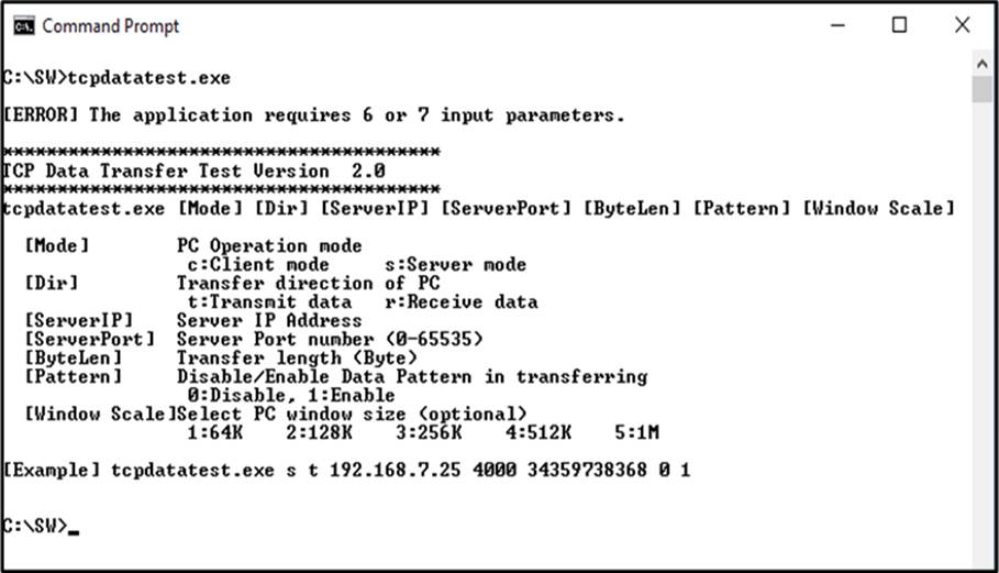
Figure 4‑1 “tcpdatatest” application usage
The “tcpdatatest” application is executed to send or receive TCP data on a PC. It requires six mandatory parameters and one optional parameter. It is important to ensure that the parameter inputs match those set on the FPGA. The details of each parameter are as follows.
Mandatory parameters
1) Mode : c – The PC runs in Client mode and the FPGA runs in Server mode
s – The PC runs in Server mode and the FPGA runs in Client mode
2) Dir : t – transmit mode (the PC sends data to the FPGA)
r – receive mode (the PC receives data from the FPGA)
3) ServerIP : The IP address of the FPGA when the PC runs in Client mode
(Default is 192.168.100.42)
4) ServerPort : The port number of the FPGA when the PC runs in Client mode
(Default is 60000)
5) ByteLen : The total size of data to be transferred in bytes. This parameter is used
only in transmit mode only and is ignored in receive mode. In transmit
mode, the ByteLen value must match the total transfer size set in the
receive data test menu of the FPGA. In receive mode, the application
is closed when the connection is terminated.
6) Pattern : 0 – Generate dummy data in transmit mode and disable data verification
in receive mode.
1 – Generate incremental data in transmit mode and enable data
verification in receive mode.
Optional parameter
1) Window Scale : Indicate the size of the allocated buffer for the TCP socket on PC.
It is also applied for TCP Window scaling feature. The valid range is 1-5.
1 – Allocated buffer size of 64 Kbyte
2 – Allocated buffer size of 128 Kbyte
3 – Allocated buffer size of 256 Kbyte
4 – Allocated buffer size of 512 Kbyte
5 – Allocated buffer size of 1 Mbyte
The sequence of the test application when running in transmit mode and receive mode are described as follows.
1) Obtain and verify the user’s input parameters, excluding the optional one.
2) Create a socket, set the socket options, and specify the socket memory size.
3) Establish a new connection using the server IP address and server port number.
4) Allocate 2 MB memory for the send buffer.
5) Generate the incremental test pattern to the send buffer if the dummy pattern is not selected.
6) Send the data out and read the total amount of sent data through the socket function.
7) Calculate the remaining transfer size.
8) Print the total transfer size every second.
9) Repeat step 5) – 8) until the remaining transfer size is 0.
10) Calculate the total performance and print the result on the console.
11) Close the socket and free the memory.
Receive mode
1) Follow the step 1) – 3) of the Transmit data mode.
2) Allocate 2 MB memory for the receive buffer.
3) Wait for the data to be stored in the receive buffer and read it, and increase the total amount of received data.
4) Verify the received data by the incremental pattern if the data verification is enabled. Otherwise, skip this step. Print an error message if the data is incorrect.
5) Print the total amount of received data every second.
6) Repeat steps 3) – 5) until the connection is closed by the other device.
7) Calculate the total performance and print the result on the console.
8) Close the socket and free the memory.
4.2 “tcp_client_txrx_xg” for full duplex test
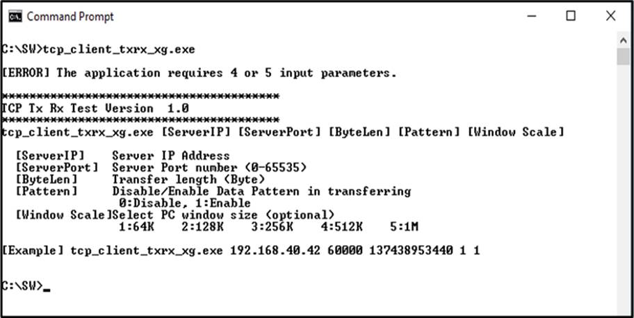
Figure 4‑2 “tcp_client_txrx_xg” application usage
The “tcp_client_txrx_xg” application enables PC to send and receive TCP data through Ethernet using the same port number simultaneously. It runs only in Client mode and requires server parameters (network parameters of TOE100G-IP) to be input by the user. The application uses five parameters, described as follows.
Mandatory parameters
1) ServerIP : The IP address of the FPGA
2) ServerPort : The port number of FPGA
3) ByteLen : The total transfer size in byte units, which is the total amount of
transmitted data and received data. This value must be equal to the
transfer size set on the FPGA for running full-duplex test.
4) Pattern : 0 – Generate dummy data for the sending function and disable data
verification for the receiving function. This mode is used to check the
best performance of full-duplex transfer.
1 – Generate incremental data for the sending function and enable data
verification for the receiving function.
Optional parameter
1) Window Scale : Indicate the size of the allocated buffer for the TCP socket on PC.
It is also applied for TCP Window scaling feature. The valid range is 1-5.
1 – Allocated buffer size of 64 Kbyte
2 – Allocated buffer size of 128 Kbyte
3 – Allocated buffer size of 256 Kbyte
4 – Allocated buffer size of 512 Kbyte
5 – Allocated buffer size of 1 Mbyte
Note: Window Scale parameter is an optional. If the user does not provide this parameter, it is automatically set to 1.
The sequence of the test application is as follows.
1) Obtain and verify the user’s input parameters, excluding the optional one.
2) Allocate 2 MB memory for the send and receive buffers, separately.
3) Create the socket, set socket options, and set the socket memory size.
4) Create a new connection using the server IP address and server port number.
5) If the test pattern is enabled, generate the incremental test pattern in the send buffer; otherwise, skip this step for dummy data.
6) If the send function is not ready for operating, skip this step; otherwise, continue the following steps.
i) If the test pattern is enabled, generate the incremental test pattern in the send buffer; otherwise, skip this step for dummy data.
ii) Send the data out and read the amount of sent data through socket function.
iii) Calculate the remaining send size.
7) If the receive function is not ready for operating, skip this step; otherwise, continue the following steps.
i) Read the data from the receive buffer and increase the total amount of received data.
ii) If the test pattern is enabled, verify the received data using the incremental pattern, and print an error message if verification fails; otherwise, skip this step.
8) Print the total amount of transmitted data and received data every second.
9) Repeat steps 5) – 8) until the total amount of transmitted and received data equals ByteLen, set by the user.
10) Calculate the performance and print the result on the console.
11) Close the socket.
12) Sleep for 1 second to wait until the hardware to complete the current test loop.
13) Start a new test by repeating steps 3) – 12) in forever loop. However, if the data verification fails, stop the application.
5 Revision History
|
Revision |
Date |
Description |
|
2.1 |
25-May-23 |
Correct Figure 2‑4. |
|
2.0 |
16-May-23 |
1) Change full-duplex test application to “tcp_client_txrx_xg”. 2) Update sequence of test applications. 3) Support RS-FEC in 100G Ethernet (MAC) Subsystem. 4) Update link for the details 5) Update USER_FFSTS_INTREG register in [19:6] following the update of TCPRxFfRdCnt. 6) Update the step of Receive data test. 7) Add USER_INT_INTREG to register map and update firmware to use Connection interrupt. |
|
1.1 |
11-Mar-22 |
Update EMAC to be hard IP and soft IP |
|
1.0 |
16-Apr-21 |
Initial version release |