TOE10G-IP with CPU reference design
2.1.2 10G/25G Ethernet Subsystem
2.1.3 Versal Multirate Ethernet MAC Subsystem
3.6 Function List in User Application
4.1 �tcpdatatest� for Half Duplex Test
4.2 �tcp_client_txrx_xg� for Full Duplex Test
1 Introduction
The TCP/IP protocol suite, which is the foundation of network applications, consists of four layers: Application, Transport, Internet, and Network Access. Figure 1‑1 demonstrates how the Network Access layer is split into two sublayers: Link and Physical, aligning with the hardware implementation using an FPGA.
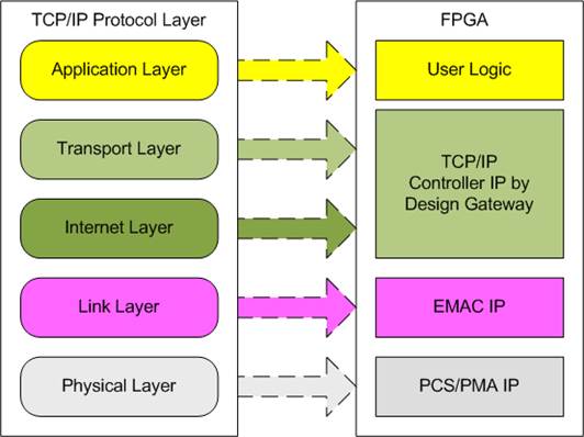
Figure 1‑1 TCP/IP Protocol Layer
The PCS and PMA modules are provided by AMD Xilinx at no charge for each FPGA, while the Ethernet MAC (EMAC) module can be implemented through several solutions such as the 10G25GEMAC-IP from Design Gateway, the 10G/25G Ethernet Subsystem from AMD Xilinx, and the Versal Multirate Ethernet MAC (the Hard IP).
The TOE10G-IP implements the Transport and Internet layers of the TCP/IP Protocol using dedicated hardware logic, eliminating the need for a CPU or DDR memory. This design enables efficient processing of TCP payload data through the user interface of TOE10G-IP. TOE10G-IP is responsible for constructing Ethernet packets, embedding the TCP payload data form the user, and transmitting it to the EMAC. If the user�s data exceeds the size limit for a single Ethernet packet, TOE10G-IP will split the data across multiple packets. To create a complete Ethernet packet, the TOE10G-IP processes and appends the TCP/IP header before transmission. On the other hand, when TOE10G-IP receives an Ethernet packet from the EMAC, it extracts and verifies the packet�s content. If valid, TOE10G-IP extracts the TCP payload data and forwards it to the user logic; otherwise, the packet is discarded.
The reference design comprises a simple user logic, TOE10G-IP, and a 10G Ethernet Subsystem for TCP/IP data transfer. The data can be exchanged with the target device, which could be a PC or another FPGA integrating with TOE10G-IP. Design Gateway provides two test applications for the PC to evaluate the demo using a single TCP session: �tcpdatatest� for half-duplex (send or receive data) and �tcp_client_txrx_xg� for full-duplex (simultaneous send and receive) operations.
To facilitate flexible testing, the user can set test parameters and control the TOE10G-IP demo operation via a UART interface integrated into a CPU system. The user can monitor the current status and adjust test parameters through the console. The CPU firmware is built using a simple bare-metal OS. Detailed information about the demo is provided in the sections below.
2 Hardware
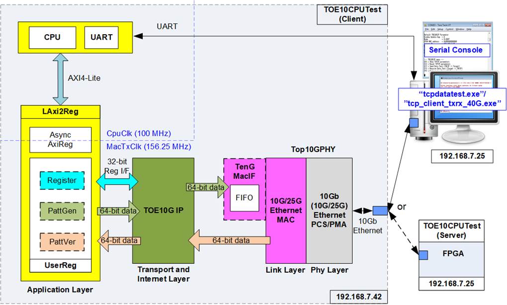
Figure 2‑1 Demo Block Diagram
In the test system (TOE10CPUTest), the TOE10G-IP connects to an Ethernet Subsystem to establish a 10G Ethernet link with the target device. This document outlines various Ethernet Subsystem solutions such as the 10G25GEMAC-IP from Design Gateway and the 10G/25G Ethernet Subsystem from AMD Xilinx. Some solutions may require adapter logic blocks (MACTxIF and MACRxIF) to interface between the TOE10G-IP and the Ethernet Subsystem, which will be further explained in the subsequent sections.
The user interface of the TOE10G-IP connects to the UserReg module, which performs three functions corresponding to three user interfaces of TOE10G-IP: Register files for the Register interface, PattGen for generating and sending test data via the Tx FIFO interface, and PattVer for verifying received data via the Rx FIFO interface. The CPU configures the Register files, PattGen, and PattVer submodules through the AXI4-Lite bus.
Additionally, the processor system allows the user to configure test parameters via a Serial console and monitor test progress and system status. Command execution sequences are managed by the CPU firmware, providing enhanced user interaction and control over the testing procedures.
The reference design generally operates with two clock domains: CpuClk and MacClk, with MacClk typically sourced from the Ethernet Subsystem running at 156.25 MHz. For systems using the Versal Multirate Ethernet MAC Subsystem (MRMAC - the hard IP on Versal devices), the Ethernet Subsystem�s clock domain is set to 322.265625 MHz. In such cases, adapter logic blocks (MACTxIF and MACRxIF) are required to manage data transfer across different clock domains between MacClk and UserClk. The LAxi2Reg module incorporates asynchronous logic to handle clock domain crossings between CpuClk and MacClk/UserClk.
2.1 Ethernet Subsystem
The Ethernet Subsystem operates across multiple protocol layers, including the MAC (Media Access Control), PCS (Physical Coding Sublayer), and PMA (Physical Medium Attachment) layers. These layers work for interface with external devices using the 10G BASE-R standard. The TOE10G-IP communicates with the Ethernet MAC via a 64-bit AXI4-stream interface clocked at 156.25 MHz. When the TOE10G-IP interface does not align with the 10G Ethernet MAC interface, adapter logic is used to ensure proper operation.
This document presents three different Ethernet Subsystem implementations: the DG 10G25GEMAC-IP, the 10G/25G Ethernet Subsystem (Soft IP) from AMD Xilinx, and the Multirate Ethernet MAC Subsystem (Hard IP). Detailed descriptions of each solution are provided below.
2.1.1 DG 10G25GEMAC-IP
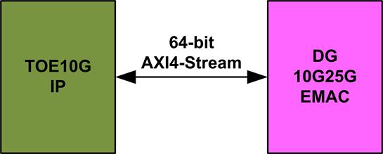
Figure 2‑2 Ethernet Subsystem using DG 10G25GEMAC-IP
This configuration minimizes FPGA resource utilization by allowing the TOE10G-IP to connect directly with the DG 10G25GEMAC-IP, eliminating the need for additional adapter logic. The Ethernet Subsystem is composed of two separate IP cores: DG 10G25GEMAC-IP and 10G Ethernet PCS/PMA.
DG 10G25GEMAC-IP
This IP core implements the Ethernet MAC layer with a 64-bit interface running at 156.25 MHz, making it suitable for 10G Ethernet operations. It directly interfaces between the TOE10G-IP and the 10G Ethernet PCS/PMA from AMD Xilinx without requiring additional logic. Further details can be found on the Design Gateway website.
https://dgway.com/products/IP/GEMAC-IP/dg_10g25gemacip_data_sheet_xilinx/
10G Ethernet PCS/PMA (10GBASE-R)
The 10G Ethernet PCS/PMA (10GBASE-R) is a no-charge IP core provided by AMD Xilinx. It features a 64-bit XGMII interface operating at 156.25 MHz, designed for 10G Ethernet speed. More information is available on the AMD Xilinx website.
https://www.xilinx.com/products/intellectual-property/10gbase-r.html
The reference design configuration settings for the 10G Ethernet PCS/PMA IP core using the IP wizard are as follows.
· General/ Select Core : Ethernet PCS/PMA 64-bit
· General/ Speed : 10.3125G
· PCS/PMA Option/ Base-R/KR Standard : BASE-R
· User Interface/ Control and Statistics Interface : Control and Status Vectors
2.1.2 10G/25G Ethernet Subsystem

Figure 2‑3 Ethernet Subsystem using 10G/25G Ethernet Subsystem (Soft IP)
The 10G/25G Ethernet Subsystem from AMD Xilinx is an integrated solution that combines a 10G Ethernet MAC with a PCS/PMA in BASE-R mode, specifically designed for use with UltraScale and UltraScale+ FPGAs. Although the signal names of the TOE10G-IP and the 10G/25G Ethernet Subsystem are compatible, there are notable differences in the behavior of the �valid� and �ready� signals.
The TOE10G-IP requires uninterrupted packet transfer from the start to the end of a data packet, meaning the �valid� and �ready� signals must remain asserted to 1b throughout the packet transfer. In contrast, when connecting to 10G Ethernet connection, the 10G/25G Ethernet Subsystem may de-assert the �ready� signal to pause packet transmission before the final data of the packet is transmitted. This difference necessitates the use of Tx adapter logic (MAC64bTxIF) to bridge the TOE10G-IP and the 10G/25G Ethernet Subsystem for transmission path. Furthermore, the 10G/25G Ethernet Subsystem can connect to 1G/10G Ethernet using Aquantia PHY for speed adjustment. In such cases, the packet transfer in both transmit and receive interface of the Ethernet Subsystem can pause before the final packet data transfer. Consequently, both MAC64bTxIF and MAC64bRxIF submodules must be integrated between the TOE10G-IP and the 10G/25G Ethernet Subsystem, as shown in Figure 2‑3.
Further details about the 10G/25G Ethernet Subsystem can be found on the AMD Xilinx website.
https://www.xilinx.com/products/intellectual-property/ef-di-25gemac.html
Additional details of MAC64bTxIF and MAC64bRxIF are described subsequently.
MAC64bTxIF

Figure 2‑4 MAC64bTxIF Block Diagram
The Tx interface characteristics of 10G/25G Ethernet Subsystem and TOE10G-IP differ. TOE10G-IP requires continuous data transmission for one packet, while the AMD Xilinx 10G/25G Ethernet Subsystem does not support this feature. The Ethernet MAC (EMAC) in the Ethernet Subsystem may de-assert the ready signal to pause data reception before the end of the packet.
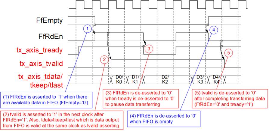
Figure 2‑5 Timing Diagram for Data Transfer from TOE10G-IP to FIFO
1) Before asserting U2MacReady to 1b for receiving a new packet from the user, two conditions must be met. First, the free space in the FIFO must be sufficient to store the maximum packet size of 9014 bytes. For simplified monitoring logic, the upper bit of FfDataCnt is read to confirm that the amount of data in the FIFO does not exceed 768 (indicating that the free space exceeds 1151 units of 64-bit data). Second, the previous packet must be completely transferred, which is indicated by U2MacReady being 0b.
2) The user starts transmitting a packet by asserting U2MacValid to 1b. The input signals from the user (U2MacData, U2MacKeep, U2MacLast, and U2MacUser) are valid and stored in the FIFO when both U2MacValid and U2MacReady are asserted to 1b. Subsequently, the inputs are stored in the FIFO by asserting rFfWrEn to 1b. The 74-bit write data to the FIFO consists of 64-bit data (U2MacData), 8-bit byte enable (U2MacKeep), end flag (U2MacLast), and error flag (U2MacUser).
3) After receiving the final data of a packet (U2MacLast=1b and U2MacValid=1b), U2MacReady is de-asserted to 0b to pause data transmission for reading FfDataCnt.
4) If FfDataCnt shows that the free space in the FIFO is sufficient, U2MacReady will be re-asserted to 1b in the next cycle.
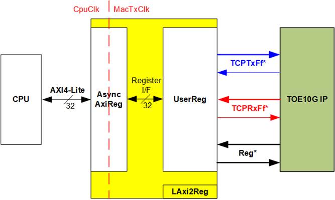
Figure 2‑6 Timing Diagram for Data Transfer from FIFO to EMAC
1) The transmission of a new packet begins when the FIFO contains some data (FfDataCnt[10:2] ≠ 0) and no packet is currently transmitting (tx_axis_tvalid=0b). To initiate data transmission, tx_axis_tvalid is set to 1b, along with the valid output signals to EMAC: 64-bit tx_axis_tdata, 8-bit tx_axis_tkeep, tx_axis_tlast, and tx_axis_tuser.
2) If data is successfully transmitted to EMAC (tx_axis_tvalid=1b and tx_axis_tready=1b), wFfRdAck is asserted to �1� to retrieve the next data from FIFO.
3) If tx_axis_tready is de-asserted to 0b, wFfRdAck will be de-asserted to 0b to pause reading new data from the FIFO. Consequently, all output signals sent to EMAC hold their values until EMAC re-asserts tx_axis_tready to 1b.
4) After the final data of a packet is completely transferred (tx_axis_tlast=1b and tx_axis_tready=1b), tx_axis_tvalid is de-asserted to 0b to pause data transmission and check the data size in FIFO for transferring the next packet.
5) The next packet is transmitted when the FIFO has enough data, returning to step 1 to transmit the new packet.
MAC64bRxIF
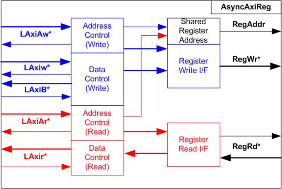
Figure 2‑7 MAC64bRxIF Block Diagram
When the 10G/25G Ethernet Subsystem is connected to the Aquantia PHY to support both 1G Ethernet and 10G Ethernet, the Rx interface of the Ethernet MAC (EMAC) inside the Ethernet Subsystem may not guarantee continuous packet data transfer, as it can de-assert the valid signal before the last packet data transmission. To address this, the MAC64bRxIF is used to buffer a complete received packet before forwarding it to the TOE10G-IP, ensuring uninterrupted packet data transmission.
The FIFO depth inside MAC64bRxIF is 4096, which is sufficient for storing several Ethernet packets. Similar to MAC64bTxIF, it is a First-Word Fall-Through (FWFT) FIFO. The �Remain Packet Counter� indicates the number of packets stored in the FIFO, increasing when a complete packet is received from EMAC and decreasing when a complete packet is forwarded to TOE10G-IP.
The operation of MAC64bRxIF is divided into two parts. The first part handles transferring a packet from EMAC to FIFO, and the second part handles transferring a packet from FIFO to TOE10G-IP. Timing diagrams of each part are displayed in Figure 2‑8 and Figure 2‑9.

Figure 2‑8 Timing Diagram for Data Transfer from EMAC to FIFO
1) Read FfDataCnt to check the available free space in the FIFO. If FfDataCnt is less than 2944 (indicating that the free space in FIFO exceeds 1153), it is sufficient to store the maximum packet size of 9014 bytes. Additionally, rPacTrans must be equal to 0 to confirm that no packet is currently being transmitted. Once these conditions are met, assert rx_axis_tready to 1b to begin data reception from EMAC.
2) When rx_axis_tvalid is asserted to 1b to indicate the start of a new packet transfer, store the data and control signals from EMAC, including 64-bit rx_axis_tdata, 8-bit rx_axis_tkeep, rx_axis_tlast, and rx_axis_tuser, in the FIFO. Assert rFfWrEn to 1b to write the 74-bit data to the FIFO.
3) After the first data of a packet is received, assert rPacTrans to 1b until the end of packet is received. This can be used to monitor the packet transmission status.
4) If the final data of a packet is received and the free space size in the FIFO is insufficient (FFDataCnt≥2944), de-assert rx_axis_tready to 0b to pause data reception.
5) After the final data of a packet is received, de-assert rPacTrans to 0b to indicate that packet transmission status has changed from Busy to Idle.
6) After storing the final data of a packet in the FIFO (rFfWrEn=1b and rFfWrData[72]-last flag = 1b), increment rPacCnt, the counter that shows the total number of packets stored in the FIFO.
7) If the next packet is received while rx_axis_tready is still de-asserted to 0b, the received packet will be dropped and not be stored in the FIFO.
8) Re-assert rx_axis_tready to 1b when no packet is being transmitted and there is sufficient free space size in the FIFO.

Figure 2‑9 Timing Diagram for Data Transfer from FIFO to TOE10G-IP
1) Before initiating the transfer of a packet from FIFO to TOE10G-IP, ensure that at least one packet is stored in FIFO (rPacCnt>0) and data transmission is not paused (rRdPause= 0b). If both conditions are met, packet forwarding begins by setting rFfRdAck to 1b, which remains active until the final data of the packet is transferred.
2) To optimize timing constraints, the data output from the FIFO is first routed through D Flip-Flops being forwarded to the Mac2U I/F. As s result, Mac2UValid is set to 1b on the clock cycle following the assertion of rFfRdAck[0]. Additionally, Mac2UData, Mac2UKeep, and Mac2ULast are set to the values from FfRdData[63:0], FfRdData[71:64], and FfRdData[72], respectively.
3) After the final data of a packet is read (rFfRdAck[0]=1b and rFfRdData[72]=1b) and forwarded, the TOE10G-IP requires a two-clock cycle pause. By asserting rRxPause to 1b for a single clock period, Mac2UValid is set to 0b to pause packet transmission for two clock cycles. At the same time, rPacCnt is decremented.
4) Once rRdPause is de-asserted, return to step 1) by checking the remaining packet in the FIFO, indicated by rPacCnt. If a new packet is found, packet transmission can be restarted by setting rFfRdAck[0] to 1b.
2.1.3 Versal Multirate Ethernet MAC Subsystem
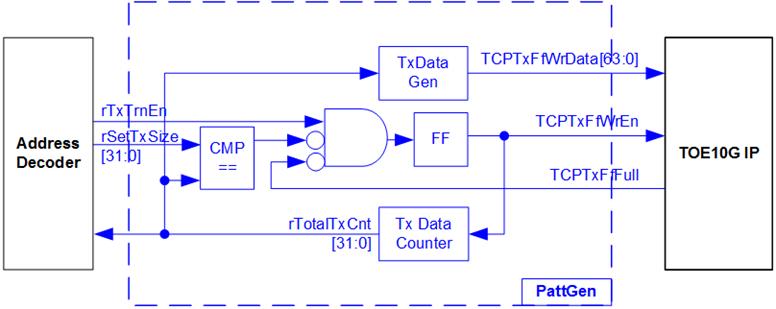
Figure 2‑10 Ethernet Subsystem using MRMAC
The Multirate Ethernet MAC (MRMAC) is a versatile integrated Hard IP available in Versal device. It co-operates with the transceiver module to complete both MAC and PHY functionalities for 10G Ethernet operations. Further information of this Hard IP can be found on the AMD Xilinx website.
https://www.xilinx.com/products/intellectual-property/mrmac.html
MRMAC configuration in the reference design:
· MRMAC Configuration Preset : 4x10GE Wide
· MRMAC Mode : MAC+PCS
· AXI Datapath Interface : Independent 32b Non-Segmented
To bridge the TOE10G-IP, which operates with a 64-bit AXI4-ST interface at 156.25 MHz, with the MRMAC, which uses a 32-bit AXI4-ST at 322.265625 MHz, specific adapter logics are required. These adapters, MACTxAsync64to32IF and MACRxAsync32to64IF, handle both clock domain crossing and data width conversion, enabling seamless communication between the TOE10G-IP and the MRMAC.
MACTxAsync64to32IF
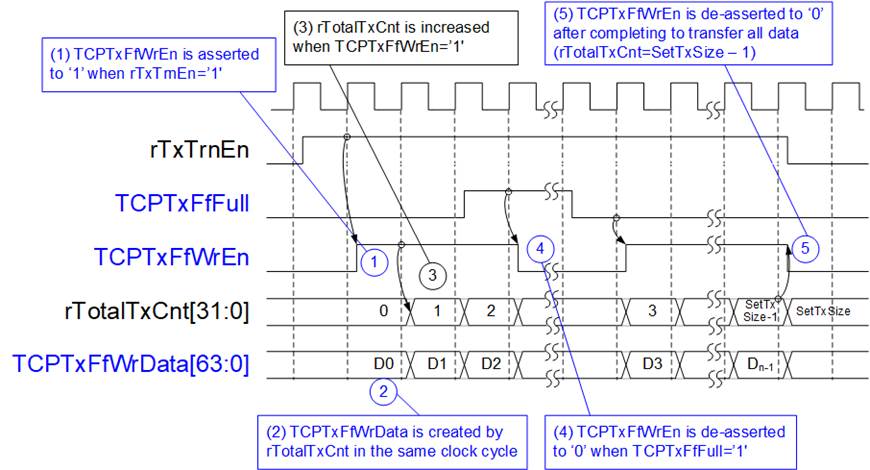
Figure 2‑11 MACTxAsync64to32IF Logic Diagram
This module facilitates asynchronous data transfer from the 64-bit AXI4 stream interface (operating in the UserClk domain) of the TOE10G-IP to the 32-bit AXI4 stream interface (operating in the MacClk domain) of the Versal Multirate Ethernet MAC Subsystem. To effectively manage data flow, the module employs two First-Word Fall-Through (FWFT) FIFOs: one for buffering the input stream (TxFf). The module�s functionality is divided into two primary operations: writing to and reading from the FIFOs.
For the Write operation, the UserClk frequency must be at least 156.25 MHz to support the 10G Ethernet transfer rate. As data is transmitted, the FIFO may reach capacity, which requires pausing the write operation. The write data count of both TxFf and PacFf is monitored to ensure sufficient space for upcoming packet transfers. If space is insufficient, U2MacReady is de-asserted to 0b, pausing the incoming data stream. Once the last packet data is stored in TxFf (indicated by U2MacLast being set to 1b), dummy data is written to PacFf to signal the completion of packet storage.
For the Read operation, the read operation begins by setting wTxFfRdAck to 1b, initiating data retrieval from TxFf when all data of a packet is available. This is monitored by PacFfRdEmpty and TxFfRdEmpty. Reading from the FIFO only begins if no previous packet data is still being transferred (indicated by MacTxValid being 0b) or when the last packet�s data has been successfully transferred (indicated by both MacTxReady and MacTxLast being set to 1b). Data from TxFf (TxFfRdData) is loaded to shift registers and transmitted to the MRMAC over two clock cycles, converting the 64-bit data into two 32-bit segments. This data is continuously transferred until the packet is fully transmitted. rMacTxDataH indicates whether the current data transfer to the MRMAC is for the lower or the upper 32-bit data set. It is set to 1b when transmitting the upper 32-bit data set.
The status signal, r1stRead, is set to 1b when the next data read from TxFf is the first packet data. This signal controls when wTxFfRdAck is set to 1b. When the last data is read from TxFf, wPacFfRdAck is set to 1b for a single clock cycle to clear the dummy data in PacFf.
MacTxValid is controlled by an S-R FF and remains asserted at 1b throughout the packet transfer. It is de-asserted after the last data transfer is completed.
For more illustration, the timing diagram of the Read operation is depicted in Figure 2‑12
Figure 2‑12 MACTxAsync64to32IF Timing Diagram
1) During the idle state, when MacTxValid is 0b, a new packet transfer can be initiated once all initial conditions are met: r1stRead is set to 1b (indicating the start of a new packet), and both PacFfRdEmpty and TxFfRdEmpty are 0b (indicating all data of the subsequent packet is available in TxFf). wTxFfRdAck is set to 1b for the first data read, followed by setting MacTxValid to 1b in the subsequent clock cycle to initiate packet transfer. MacTxValid remains at 1b throughout the transfer to ensure continuous transmission of all data within the packet until the last data is transmitted.
2) Assume the first packet includes three data units (D0, D1, and D2). The last flag (TxFfRdData[72]) remains at 0b for the first two data cycles. After the first data is read, r1stRead resets to 0b. wTxFfRdAck can be asserted again when data is present in TxFf (TxFfRdEmpty=0b) and after the upper 32-bit data has been completely transferred (MacTxReady=1b and rMacTxDataH=1b).
3) Since TxFf is the FWFT type, the read data (TxFfRdData) is immediately valid in the same cycle when wTxFfRdAck is set to 1b. Upon assertion of wTxFfRdAck, rMacTxData[63:32] and MacTxData[31:0] are loaded from TxFfRdData[63:0]. The last flags for each 32-bit data sets (rMacTxLast[1] and MacTxLast) are decoded from TxFfRdData[72] (last flag) and TxFfRdData[68] (flag indicating that the number of valid bytes in rMacTxData exceeds 4).
4) Once the data is successfully transferred (MacTxReady=1b), MacTxData and MacTxLast are loaded from rMacTxData[63:32] and rMacTxLast[1], respectively. Additionally, rMacTxDataH toggles to 1b to indicate the current MacTxData contains the upper 32 bits of the 64-bit data. This toggle occurs when MacTxReady is set to 1b.
5) If MacTxReady is de-asserted to 0b during a packet transfer, wTxFfRdAck is immediately set to 0b, pausing the read operation and preserving the current values of MacTxData and MacTxLast.
6) Upon reading the last data from TxFf (indicated by both wTxFfRdAck and TxFfRdData[72] being set to 1b), wPacFfRdAck is set to 1b for a single clock cycle to flush one dummy data from PacFf, reducing the packet count in TxFf and resetting r1stRead to 1b, preparing for the first data read of the next packet.
7) After the successful transmission of the last data (with MacTxReady and MacTxLast both set to 1b), a new packet transfer can be initiated when conditions permit (PacFfRdEmpty and TxFfRdEmpty both set to 0b and r1stRead=1b), iterating to step 1). In this case, wTxFfRdAck is set to 1b during the first data transfer. If the new packet contains only 32-bit data, MacTxLast is set to 1b during the first data transmission, with r1stRead remaining set to 1b after the first read is completed.
MACRxAsync32to64IF
The MacRxAsync32to64IF serves as an adapter for packet transfers from the MRMAC, which operates with a 32-bit AXI4 Stream interface at 322.266 MHz, to the TOE10G-IP, that utilizes a 64-bit AXI4 Stream interface at 156.25 MHz. This adapter manages the differences in clock domains and data bus widths between the two systems. It includes logic for clock-crossing from the MacClk domain to the UserClk domain and for converting data from 32 bits to 64 bits.
While the MRMAC�s output may occasionally pause during any transfer cycle, the TOE10G-IP requires continuous data transfer within each packet. To manage this requirement, the MACRxAsync32to64IF employs an RxFf (FWFT FIFO) to buffer incoming packet data. This data is validated by Error Detection logic before proceeding.
Additionally, a second FWFT FIFO, PacFf, stores dummy data that marks the end of packet written to the RxFf. The FIFO count of PacFf is then used to track and indicate the number of packets stored in RxFf, facilitating data management for retrieval.
As illustrated in Figure 2‑13, the internal logic of the MacRxAsync32to64IF is divided into two groups: the Write FIFO and the Read FIFO. The details of both are explained below.
Figure 2‑13 MacRxAsync32to64IF Logic Diagram
The Error Detection logic continuously monitors the full status of both the RxFf and PacFf through their write data counter outputs. If either FIFO approaches the full threshold, the Error Detection logic halts data writing, asserts an error flag, and sets the last flag, indicating that an error has occurred in the current packet. Any remaining data in the packet is then discarded. Data writing resumes only once sufficient space becomes available in both FIFOs and a new packet is received.
The Write Controller is responsible for converting data from 32 bits to 64 bits. Typically, the RxFf is written after receiving two 32-bit inputs, except when processing the last packet data. If only 32 bits are received, the last data is written to RxFf along with dummy data to maintain alignment. Additionally, the PacFf is written during the last data transfer cycle, signaled when both rRxFfWrEn and rRxFfWrData[72] are set to 1b, marking the end of a data packet.
On the Read side, the process starts by setting rRxFfRdAck to 1b, which initiates the reading of the first data of each packet from RxFf. This action occurs only when the entire packet is confirmed to be available in RxFf, indicated by PacFfRdEmpty and RxFfRdEmpty both being 0b. Once data reading begins, rRxFfRdAck remains asserted until the last packet data is read (marked by RxFfRdData[72]=1b). After reading the last data, rRxFfRdAck is de-asserted for two clock cycles, a requirement by the TOE10G-IP to allow a brief pause after the last packet data. Once another packet is ready, rRxFfRdAck can be re-asserted to 1b.
The detailed operations of the Error Detection and the Write Controller functionalities are depicted in Figure 2‑14 and Figure 2‑15, respectively.

Figure 2‑14 Error Detection of MacRxAsync32to64IF Timing Diagram
1) During the Write side operation, the available space in both RxFf and PacFf is continuously monitored using RxFfWrCnt and PacFfWrCnt. In a normal scenario, as the input stream is received, it is synchronized into DFFs. For example, MacRxData is loaded into rMacRxData. When rDiscardEn[0] is set to 0b, indicating a normal scenario, the data stream from the DFFs is routed to the Write Controller with rRxValid set to 1b, allowing the data stream to proceed.
2) The value of rRxValid is directly linked to MacRxValid, and includes a two-clock cycle latency during transitioning between 1b and 0b. This delay accounts for the required synchronization before the Write Controller can process the data.
3) If the FIFO space reaches a critical threshold, both rFfAFull and rDiscardEn[0] are set to 1b. This condition triggers the cessation of the current data stream being forwarded to the Write Controller. Simultaneously, rRxValid, rRxLast, and rRxError are set to 1b, marking the last cycle of this packet and indicating an error status. Following this, the incoming data of the current packet (e.g., Dn2 and Dn3) is no longer forwarded to the Write Controller, effectively halting further data processing.
4) Upon detecting the end of the current packet, signaled by MacRxLast being set to 1b, the dropped packet function is disabled by de-asserting rDiscardEn[0] to 0b. This action resets the logic, preparing the system for the next packet and allowing the system to resume normal operation without retaining the error state.
Figure 2‑15 Write Controller of MacRxAsync32to64IF Timing Diagram
1) The initial value of rWordHEn, which indicates whether the 32-bit received data is the lower or upper word, is set to 0b at the start of a new packet. Upon receiving the first 32-bit packet data (rRxData[31:0]), along with rRxKeep[3:0], they are loaded into the lower part of rRxFfWrData (bits[31:0] and bits[67:64]). Afterward, rWordHEn is toggled after each data receipt, as indicated by rRxValid being set to 1b.
2) In the next data cycle, where both rWordHEn and rRxValid are set to 1b, the incoming 32-bit data, along with its corresponding control bits, are loaded into the upper part of rRxFfWrData (bits[63:32] and bits [71:68]). During this cycle, rRxFfWrEn is set to 1b, enabling the writing of the complete 64-bit data into the FIFO.
3) When the last data of a packet is received, as indicated by both rRxValid and rRxLast being set to 1b, rRxFfWrEn is always set to 1b to write the data into the FIFO, regardless of the state of rWordHEn. If only the lower data has been received (rWordHEn=0b), the remaining 4 bits of the Keep value for the upper data are set to zero to ensure proper alignment. This guarantees that the data is correctly stored in the FIFO, even when only the lower portion of the data is available.
2.2 TOE10G-IP
https://dgway.com/products/IP/TOE10G-IP/dg_toe10gip_data_sheet_xilinx_en/
2.3 CPU and Peripherals
In the reference design, the CPU system is extended with an additional peripheral to access the test logic. Therefore, the hardware logic must support the AXI4-Lite bus standard to allow for CPU-initiated write and read operations. The LAxi2Reg module facilitates this connection, as shown in Figure 2‑16.

Figure 2‑16 LAxi2Reg Block Diagram
The LAxi2Reg module consists of two submodules: AsyncAxiReg and UserReg. AsyncAxiReg converts AXI4-Lite signals into a simple Register interface with a 32-bit data bus size, similar to AXI4-Lite standard. Additionally, it includes asynchronous logic to handle clock domain crossing between CpuClk and MacClk domains.
UserReg contains the Register file for parameters and status signals associated with the test logic, including TOE10G-IP. Both the data and control interfaces of TOE10G-IP are connected to UserReg.
Further details on the operations of AsyncAxiReg and UserReg are provided in subsequent sections.
2.3.1 AsyncAxiReg
Figure 2‑17 AsyncAxiReg Interface
The signals on AXI4-Lite bus interface are divided into five groups: LAxiAw* (Write address channel), LAxiw* (Write data channel), LAxiB* (Write response channel), LAxiAr* (Read address channel), and LAxir* (Read data channel). For more information on designing custom logic for the AXI4-Lite bus, refer to the following documentation.
In accordance with the AXI4-Lite standard, the write and read channels operate independently, with separate control and data interfaces for each channel. Therefore, the logic inside AsyncAxiReg that interfaces with the AXI4-Lite bus is divided into four functional groups: Write control logic, Write data logic, Read control logic, and Read data logic, as depicted on the left side of Figure 2‑17. The Write control I/F and Write data I/F of the AXI4-Lite bus are latched and then transferred to the Write register interface via clock domain crossing registers. Similarly, the Read control I/F of the AXI4-Lite bus is latched and transferred to the Read register interface. The data returned from the Register Read I/F is transferred back to the AXI4-Lite bus by using clock domain crossing registers. In the Register interface, RegAddr is shared between write and read access, so the address is loaded from LAxiAw for write access or from LAxiAr for read access.
The simple register interface is designed to be compatible with a single-port RAM interface for write transaction. For read transaction, the Register interface is slightly modified from the RAM interface by adding RdReq and RdValid signals to control read latency. Since the address of the Register interface is shared for both write and read transactions, the user cannot perform simultaneous write and read operations. The timing diagram for the Register interface is shown in Figure 2‑18.
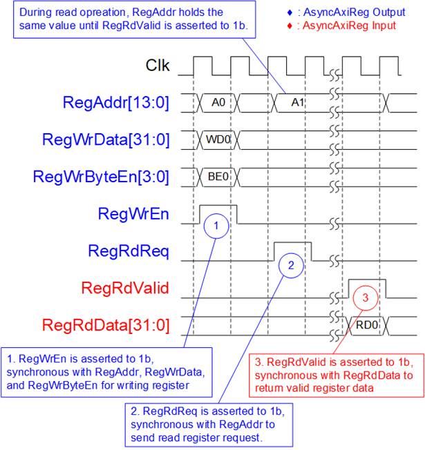
Figure 2‑18 Register Interface Timing Diagram
1) Timing diagram to write register is similar to that of a single-port RAM. The RegWrEn signal is set to 1b, along with a valid value for RegAddr (the Register address in 32-bit units), RegWrData (write data for the register), and RegWrByteEn (write byte enable). The byte enable is four bits wide, where each bit indicates the validity of a specific byte within RegWrData. For example, if RegWrByteEn[0], [1], [2], and [3] are set to 1b, then RegWrData[7:0], [15:8], [23:16], and [31:24] are valid, respectively.
2) To read from a register, AsyncAxiReg sets the RegRdReq signal to 1b, along with a valid value for RegAddr. After the read request is processed, the 32-bit data is returned. The slave detects the RegRdReq being asserted to start the read transaction. During the read operation, the address value (RegAddr) remains unchanged until RegRdValid is set to 1b. Once valid, the address is used to select the returned data through multiple layers of multiplexers.
3) The slave returns the read data on RegRdData bus by setting the RegRdValid signal to 1b. After that, AsyncAxiReg forwards the read value to the LAxir* interface.
2.3.2 UserReg
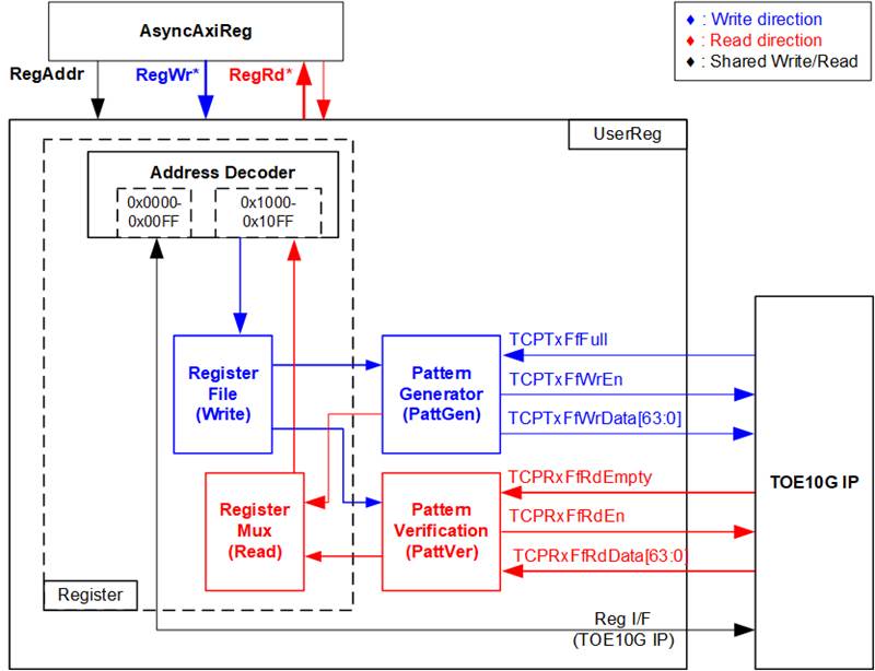
Figure 2‑19 UserReg Block Diagram
Register Block
The address range, mapped to UserReg, is split into two areas: TOE10G-IP registers (0x0000-0x00FF) and UserReg registers (0x1000-0x10FF). The Address decoder interprets the upper bits of RegAddr to select the active hardware component. Since the Register files inside UserReg are designed with a 32-bit bus size, RegWrByteEn (Write byte enable) is not used. To write data to the hardware registers, the CPU must utilize a 32-bit pointer to place a valid 32-bit value on the write data bus.
For reading from a register, a multiplexer selects the data to be returned to the CPU, based on the provided address. The lower bits of RegAddr are applied to select the active data within each Register area, while the upper bits are used to select which Register area to read from. The total read latency is one clock cycle, and the RegRdValid is created by asserting a D Flip-flop triggered by RegRdReq. Further details about the address mapping inside the UserReg module are provided in Table 2‑1.
Table 2‑1 Register map Definition
|
Address |
Register Name |
Description |
|
Wr/Rd |
(Label in the �toexgtest.c�) |
|
|
BA+0x0000 � BA+0x00FF: TOE10G-IP Register Area More details of each register are described in TOE10G-IP datasheet. |
||
|
BA+0x0000 |
TOE_RST_INTREG |
Mapped to RST register within TOE10G-IP |
|
BA+0x0004 |
TOE_CMD_INTREG |
Mapped to CMD register within TOE10G-IP |
|
BA+0x0008 |
TOE_SML_INTREG |
Mapped to SML register within TOE10G-IP |
|
BA+0x000C |
TOE_SMH_INTREG |
Mapped to SMH register within TOE10G-IP |
|
BA+0x0010 |
TOE_DIP_INTREG |
Mapped to DIP register within TOE10G-IP |
|
BA+0x0014 |
TOE_SIP_INTREG |
Mapped to SIP register within TOE10G-IP |
|
BA+0x0018 |
TOE_DPN_INTREG |
Mapped to DPN register within TOE10G-IP |
|
BA+0x001C |
TOE_SPN_INTREG |
Mapped to SPN register within TOE10G-IP |
|
BA+0x0020 |
TOE_TDL_INTREG |
Mapped to TDL register within TOE10G-IP |
|
BA+0x0024 |
TOE_TMO_INTREG |
Mapped to TMO register within TOE10G-IP |
|
BA+0x0028 |
TOE_PKL_INTREG |
Mapped to PKL register within TOE10G-IP |
|
BA+0x002C |
TOE_PSH_INTREG |
Mapped to PSH register within TOE10G-IP |
|
BA+0x0030 |
TOE_WIN_INTREG |
Mapped to WIN register within TOE10G-IP |
|
BA+0x0034 |
TOE_ETL_INTREG |
Mapped to ETL register within TOE10G-IP |
|
BA+0x0038 |
TOE_SRV_INTREG |
Mapped to SRV register within TOE10G-IP |
|
BA+0x003C |
TOE_VER_INTREG |
Mapped to VER register within TOE10G-IP |
|
BA+0x0040 |
TOE_DML_INTREG |
Mapped to DML register within TOE10G-IP |
|
BA+0x0044 |
TOE_DMH_INTREG |
Mapped to DMH register within TOE10G-IP |
|
BA+0x1000 � BA+0x10FF: UserReg control/status |
||
|
BA+0x1000 |
Total Transmit Length |
Wr [31:0] � Total transmit size in Qword units (64-bit). Valid values range from 1 to 0xFFFFFFFF. Rd [31:0] � Current transmit size in Qword units (64-bit). The value is cleared to 0 when the USER_CMD_INTREG is written by the user. |
|
Wr/Rd |
(USER_TXLEN_INTREG) |
|
|
BA+0x1004 |
User Command |
Wr [0] � Start transmitting. Set to 0b to start the transmission. [1] � Data verification enable (0b: Disable data verification, 1b: Enable data verification) Rd [0] � Transmit busy (0b: Idle, 1b: Transmit module is busy) [1] � Data verification error (0b: Normal, 1b: Error) This bit is auto-cleared when user starts new operation or reset. [2] � Mapped to ConnOn signal from TOE10G-IP |
|
Wr/Rd |
(USER_CMD_INTREG) |
|
|
BA+0x1008 |
User Reset |
Wr [0] � Reset signal. Set to 1b to reset the logic. This bit is auto-cleared to 0b. [8] � Set to 1b to clear the latched value of TimerInt. Rd [8] � Latched value of TimerInt output from the IP (0b: Normal, 1b: TimerInt assertion detected) This flag is cleared by a system reset or by setting USER_RST_INTREG[8] to 1b. [16] � Ethernet linkup status from Ethernet MAC (0b: Not linkup, 1b: Linkup) |
|
Wr/Rd |
(USER_RST_INTREG) |
|
|
BA+0x100C |
User FIFO Status |
Rd [2:0] - Mapped to TCPRxFfLastRdCnt signal of TOE10G-IP [15:3] - Mapped to TCPRxFfRdCnt signal of TOE10G-IP [24] - Mapped to TCPTxFfFull signal of TOE10G-IP |
|
Rd |
(USER_FFSTS_INTREG) |
|
|
Address |
Register Name |
Description |
|
Wr/Rd |
(Label in the �toexgtest.c�) |
|
|
BA+0x1000 � BA+0x10FF: UserReg control/status |
||
|
BA+0x1010 |
Total Receive Length |
Rd [31:0] � Current receive size from TOE10G-IP in Qword unit (64-bit). The value resets to 0 when the USER_CMD_INTREG is written by user. |
|
Rd |
(USER_RXLEN_INTREG) |
|
|
BA+0x1020 |
Connection Interrupt |
Wr[0] � Set to 1b to clear the connection interrupt (USER_INT_INTREG[0]) Rd[0] � Indicate whether an interrupt has been triggered by a change in the ConnOn signal. (1b: Edge of ConnOn signal detected from TOE10G-IP, 0b: No change in the ConnOn signal detected) Note: The current ConnOn signal value can be read from USER_CMD_INTREG[2]. |
|
Wr/Rd |
(USER_INT_INTREG) |
|
|
BA+0x1080 |
EMAC IP Version |
Rd[31:0] � Mapped to IPVersion output from DG 10G25GEMAC-IP when it is integrated to the test system. |
|
Rd |
(EMAC_VER_INTREG) |
|
Pattern Generator
The logics and timing diagram of the Pattern
Generator (PattGen) are illustrated in Figure
2‑20 and Figure
2‑21, respectively.
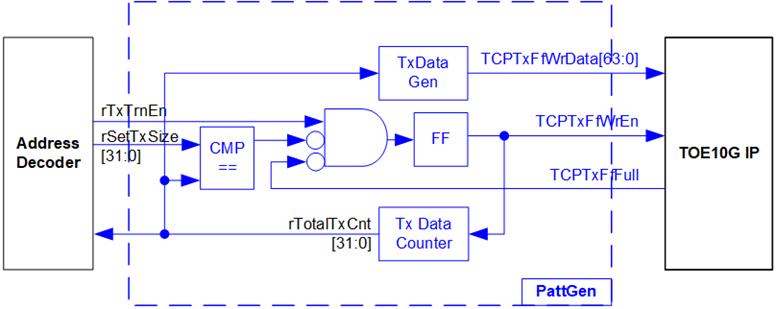
Figure 2‑20 PattGen Block
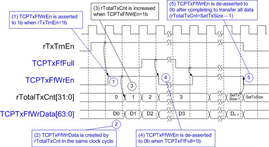
Figure 2‑21 PattGen Timing Diagram
The data counter, rTotalTxCnt, tracks the total amount of data sent to TOE10G-IP. The lower bits of rTotalTxCnt are used to generate the 32-bit incremental data for the TOETxFfWrData signal. Once the total transmitted data matches the predefined transfer size (rSetTxSize), rTxTrnEn is de-asserted to 0b, signaling the completion of the transmission.
Pattern Verification
The logics and timing diagram of the Pattern Verification (PattVer) are illustrated in Figure 2‑22 and Figure 2‑23, respectively. The verification feature is activated when the verification flag (rVerifyEn) is enabled.
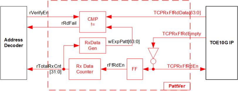
Figure 2‑22 PattVer Block
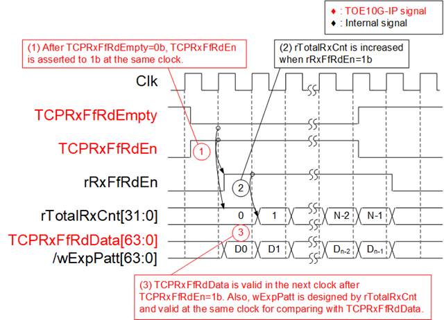
Figure 2‑23 PattVer Timing Diagram
When rVerifyEn is set to 1b, the verification logic is processed. It compares the received data (TCPRxFfRdData) with the expected pattern (wExpPatt). If the comparison fails, rRdFail is asserted to 1b, indicating a verification error. The TCPRxFfRdEn signal is created by applying a NOT operation to TCPRxFfRdEmpty, ensuring that data is read from the FIFO only when data is available.
The receive data (TCPRxFfRdData) becomes valid one clock cycle after TCPRxFfRdEn is asserted. To count the total size of the received data, rTotalRxCnt is incremented based on rRxFfRdEn, which is delayed by one clock cycle from TCPRxFfRdEn. rTotalRxCnt is applied to generate wExpPatt, which is the expected pattern for comparison with TCPRxFfRdData. Both TCPRxFfRdData and wExpPatt are valid in the same clock cycle, allowing a comparison using the rRxFfRdEn signal.
3 CPU Firmware on FPGA
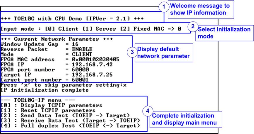
Figure 3‑1 Initialization in Client mode using Default Parameters
Figure 3‑1 illustrates the four-step process for hardware initialization.
1) Upon FPGA boot-up, the firmware polls the status of the 10G Ethernet link (USER_RST_INTREG[16]). The CPU waits until the link is established, then displays a welcome message with the IP information.
2) A menu is displayed to allow the user to select the initialization mode of the TOE10G-IP: Client, Server, or Fixed-MAC mode.
Note:
- In Client mode, TOE10G-IP sends an ARP request to obtain the MAC address of the target device from the ARP reply. In Server mode, TOE10G-IP waits for an ARP request, decodes the MAC address, and responds with an ARP reply. In Fixed-MAC mode, the user must manually set the target device�s MAC address in TOE10G-IP.
- When testing with an FPGA board and a PC, it is recommended to configure the FPGA to run in Client mode.
- When testing with two FPGA boards, three options are available for establishing the connection.
a) Set one board as Client and the other as Server.
b) Set both boards in Fixed-MAC mode.
c) Set one board to Fixed-MAC mode and the other to Client mode.
3) The CPU displays the default network parameters, including the Window update gap value, Reverse packet enable flag, initialization mode, FPGA MAC address, FPGA IP address, FPGA port number, Target IP address, and Target port number. There are two default parameter sets: Server parameter set (used for Server mode only) and Client parameter set (used for both Client and Fixed-MAC modes). When setting to Fixed-MAC mode, an additional parameter, Target MAC address, is displayed. The user can either proceed with the default parameters or update them. Instructions for changing parameters are provided in the Reset parameters menu (section 3.2).
3.1 Display parameters
This menu displays the current values of all TOE10G-IP parameters. The following steps are executed to display parameters.
1) Read the initialization mode.
Note: The Source parameters refer to the settings for the TOE10G-IP�s end inside the FPGA, while the Target parameters represent the settings for the PC or another FPGA at another end.
3) Print each parameter value on the console.
3.2 Reset parameters
This menu allows users to modify certain TOE10G-IP parameters, such as the IP address and Source port number. After setting the updated values in the TOE10G-IP registers, the CPU resets TOE10G-IP to re-initialize it with the new parameters. The CPU then monitors the busy flag until the initialization completes. The following steps are executed to reset the parameters.
1) Display all parameters on the console, following the steps in section 3.1 (Display parameters).
i) Receive the initialization mode from the user. If the mode is changed, display the parameter set of the new mode.
ii) Receive and validate each remaining parameter from the user. If an input is found to be invalid, that particular parameter will not be updated.
3) Force reset to PattGen and PattVer logics by setting USER_RST_INTREG[0] to 1b.
4) Force reset to TOE10G-IP by setting TOE_RST_INTREG[0] to 1b.
5) Set all parameters in the TOE10G-IP registers, such as TOE_SML_INTREG and TOE_DIP_INTREG.
6) De-assert the TOE10G-IP reset by setting TOE_RST_INTREG[0] to 0b to initiate the initialization process of TOE10G-IP.
7) Monitor the TOE10G-IP busy flag (TOE_CMD_INTREG[0]) and wait for the flag to de-assert to 0b, indicating that the initialization has completed.
3.3 Send data test
This test involves three user inputs: total transmit length, packet size, and connection mode (active open for Client connection mode or passive open for Server connection mode). If any input is invalid, the operation is cancelled. During the test, 32-bit incremental data is generated by the logic and sent to either a PC or another FPGA. The data is then verified by the test application on the PC or by the verification module in the FPGA. The operation is considered complete when all data is transferred from the FPGA to the PC/FPGA. The sequence of the test is as follows.
1) Receive transfer size, packet size, and connection mode from user and validate all inputs.
2) Set UserReg registers, including the transfer size (USER_TXLEN_INTREG), reset flag to clear the initial value of the test pattern (USER_RST_INTREG[0]=1b), and the command register to start the data pattern generator (USER_CMD_INTREG=0). The pattern generator in UserReg then starts sending data to TOE10G-IP.
3) Display recommended parameters for the test application on the PC by reading the current system parameters.
4) Open connection based on the connection mode setting.
i) For active open, the CPU sets TOE_CMD_INTREG to 2 (Open port). After that, it waits until the Connection interrupt status (USER_INT_INTREG[0]) is asserted to 1b. If the busy flag of TOE10G-IP (TOE_CMD_INTREG[0]) is de-asserted to 0b but the interrupt is not asserted, an error message is displayed, and the test returns to the main menu.
ii) For passive open, the CPU waits until the connection is opened by another device (PC or FPGA). The Connection interrupt status (USER_INT_INTREG[0]) is monitored until it is asserted to 1b.
5) Set the packet size in the TOE10G-IP register (TOE_PKL_INTREG) and calculate the total number of loops based on the total transfer size. The maximum transfer size for each loop is 4 GB. The operation of each loop proceeds as follows.
i) Set the transfer size of the current in the TOE10G-IP register (TOE_TDL_INTREG). The transfer size is fixed at 4 GB, except the last loop, which will equal the remaining size.
ii) Set the Send command to the TOE10G-IP register (TOE_CMD_INTREG=0).
iii) Wait until operation is completed by monitoring busy flag (TOE_CMD_INTREG[0]=0b). During this time, the CPU reads the current amount of transmitted data from user logic (USER_TXLEN_INTREG) and displays the results on the console every second.
6) Close the connection by setting the Close connection command to the TOE10G-IP register (TOE_CMD_INTREG=3). Similar to active open, the operation is considered successful when the Connection interrupt status (USER_INT_INTREG[0]) is asserted to 1b. If TOE10G-IP busy flag (TOE_CMD_INTREG[0]) is de-asserted without the Connection interrupt being asserted, an error message is displayed.
7) Calculate performance and display the test results on the console.
3.4 Receive data test
1) Receive the total transfer size, data verification mode, and connection mode from the user input. Validate all inputs.
2) Set the UserReg registers as follows.
i) Reset flag to clear the initial value of test pattern (USER_RST_INTREG[0]=1b)
ii) Data verification mode (USER_CMD_INTREG[1]=0b to only read the received data or 1b to read and verify the received data).
3) Display the recommended parameters (similar to Step 3 of Send data test).
4) Open the connection based on the connection mode (similar to Step 4 of Send data test).
5) Wait until the connection is closed by the other device (PC or FPGA). ConnOn status (USER_CMD_INTREG[2]) is monitored until it is equal to 0b. While monitoring Connon, the CPU reads the current amount of received data from the user logic (USER_RXLEN_INTREG) and displays the results on the console every second.
Note: USER_FFSTS_INTREG[15:3] is mapped from the TCPRxFfRdCnt signal of TOE10G-IP, which represents the number of 64-bit data words available in the FIFO. Therefore, the remaining unread data in the FIFO, indicated by USER_FFSTS_INTREG [2:0] (or TCPRxFfLastRdCnt), is disregarded.
7) Compare the received length from user logic (USER_RXLEN_INTREG) with the expected value from the user. If all data has been received, the CPU checks the verification result by reading USER_CMD_INTREG[1] (0b: normal, 1b: error). If any errors are detected, an error message is displayed.
8) Calculate performance and display the test results on the console.
3.5 Full duplex test
This menu facilitates full duplex testing by simultaneously transferring data between the FPGA and another device (PC or FPGA) in both directions using the same port number. The user provides four inputs: the total data size for both transfer directions, the packet size for the FPGA sending logic, the data verification mode for the FPGA receiving logic, and the connection mode (active open/close for client mode or passive open/close for server mode).
When running the test with a PC, the transfer size set on the FPGA must match the size set on the test application (tcp_client_txrx_xg). The connection mode on the FPGA must be set to passive (server mode) when running with a PC.
The test runs continuously until the user cancels the operation by entering any keys on the FPGA console and then pressing 'Ctrl+C� on the PC console. The test sequence is as follows.
1) Receive the total data size, packet size, data verification mode, and connection mode from the user and validate all inputs.
2) Display the recommended parameters for the test application running on the PC, based on the current system parameters.
3) Set the UserReg registers, including transmitted size (USER_TXLEN_INTREG), Reset flag to clear the initial value of the test pattern (USER_RST_INTREG[0]=1b), and Command register to start the data pattern generator with data verification mode
(USER_CMD_INTREG=1 or 3).
4) Open the connection following the connection mode (similar to Step 4 of Send data test).
5) Set the packet size in the TOE10G-IP register (TOE_PKL_INTREG=user input) and calculate the total transfer size for each loop. The maximum size of each loop is 4 GB. The operation of each loop proceeds as follows.
i) Set the transfer size for this loop in the TOE_TDL_INTREG register. The transfer size is fixed at 4GB which round downs to align the packet size, except for the last loop which uses the remaining size.
ii) Set the Send command to the TOE10G-IP register (TOE_CMD_INTREG=0).
iii) Wait for the Send command to complete by monitoring the busy flag (TOE_CMD_INTREG[0] =0b). While monitoring the busy flag, the CPU reads the current amount of transmitted and received data from user logic (USER_TXLEN_ INTREG and USER_RXLEN_INTREG) and displays the results on the console every second.
6) Close the connection following the connection mode.
a) For active close, the CPU waits until the total received data equals the user-specified value, then sets USER_CMD_INTREG=3 to close the connection. Next, the CPU waits for the Connection interrupt status (USER_INT_INTREG[0]=1b). If the connection fails to close (TOE_CMD_INTREG[0] or TOE10G-IP busy flag equals 0b without an interrupt), an error message is displayed.
b) For passive close, the CPU waits for the connection to be closed by the other device (PC or FPGA). The Connection interrupt status (USER_INT_INTREG[0]) is monitored until it equals 1b.
7) Check the result and any errors (similar to Step 6 and 7 of Receive data test).
8) Calculate performance and display the test results on the console. Return to Step 3 to repeat the test continuously in a loop.
3.6 Function List in User Application
This section describes the list of functions used to operate TOE10G-IP.
|
void check_ethlink(unsigned int* status) |
|
|
Parameters |
status: Returned value indicating the Ethernet status. 0: Ethernet link down, 1: Ethernet link up. |
|
Return value |
None |
|
Description |
This function reads the Ethernet MAC link status from bit 16 of the �USER_RST_INTREG� register, and returns the result through the �status� parameter. |
|
void exec_port(unsigned int port_ctl, unsigned int mode_active, unsigned int* status) |
|
|
Parameters |
port_ctl: 1-Open the port, 0-Close the port mode_active: 1-Active open/close, 0-Passive open/close status: Returned value indicating the connection status. 0: Operation successful, 1: Operation failed. |
|
Return value |
None |
|
Description |
This function initiates a connection establishment (open) or termination (close) in active mode by setting the �TOE_CMD_INTREG� register based on the �port_ctl� and �mode_active� parameters. The connection status is monitored through bit0 of the �USER_INT_INTREG� register, which indicates the Connection status interrupt. This function waits until this interrupt is asserted and then cleared the interrupt flag. |
|
void init_param(void) |
|
|
Parameters |
None |
|
Return value |
None |
|
Description |
This function reset the network parameters as described in section 3.2. It calls �show_param� to display parameters and �input_param� to receive parameters from the user. |
|
int input_param(void) |
|
|
Parameters |
None |
|
Return value |
0: Valid input, -1: Invalid input |
|
Description |
This function receives network parameters from the user, including initialization mode, Reverse packet enable, Window threshold, FPGA MAC address, FPGA IP address, FPGA port number, Target IP address, Target port number, and Target MAC address (if operating in Fixed-MAC mode). Each input is validated separately, and only valid inputs are updated. After receiving all parameters, �show_param� is called to display parameters. |
|
void int read_conon(unsigned int* status) |
|
|
Parameters |
None |
|
Return value |
status: Returned value indicating the TCP connection status 0: Connection Off, 1: Connection On |
|
Description |
This function reads bit2 of the �USER_CMD_INTREG� register to retrieve the current TCP connection status and return the result through the �status� parameter. |
|
void show_cursize(void) |
|
|
Parameters |
None |
|
Return value |
None |
|
Description |
This function displays the amount of data transmitted and received on the console. It reads the values from �USER_TXLEN_INTREG� and �USER_RXLEN_INTREG� registers, converts these values into appropriate units (bytes, Kbytes, or Mbytes), and then outputs the result on the console. |
|
void show_param(void) |
|
|
Parameters |
None |
|
Return value |
None |
|
Description |
Display the current TOE10G-IP parameters as described in section 3.1. |
|
void show_result(void) |
|
|
Parameters |
None |
|
Return value |
None |
|
Description |
This function displays the total amount of transmitted and received data. It reads the �USER_TXLEN_INTREG� and �USER_RXLEN_INTREG� registers, then reads global parameters: �timer_val� and �timer_ upper_val� to calculate the total time usage, converting the time to usec, msec, or sec units. Finally, the transfer performance is calculated and displayed in MB/s. |
|
int toe_recv_test(void) |
|
|
Parameters |
None |
|
Return value |
0: Operation is successful -1: Invalid input or error encountered |
|
Description |
Run the Receive data test as described in section 3.4. The function calls �show_cursize� during the test to display the ongoing data transfer size and �show_result� at the end of the test to display the final results. |
|
int toe_send_test(void) |
|
|
Parameters |
None |
|
Return value |
0: Operation is successful -1: Invalid input or error encountered |
|
Description |
Run the Send data test as described in section 3.3. The function calls �show_cursize� during the test to display the ongoing data transfer size and �show_result� at the end of the test to display the final results. |
|
int toe_txrx_test(void) |
|
|
Parameters |
None |
|
Return value |
0: Operation is successful -1: Invalid input or error encountered |
|
Description |
Run the Full duplex test as described in section 3.5. During the test, it calls �show_cursize� to display the ongoing data transfer size and �show_result� to display the final results. |
|
void wait_ethlink(void) |
|
|
Parameters |
None |
|
Return value |
None |
|
Description |
This function continuously reads the status of the Ethernet link by checking �USER_RST_INTREG[16]�. It waits until the Ethernet connection is successfully linked up before proceeding. |
4 Test Software on PC
4.1 �tcpdatatest� for Half Duplex Test
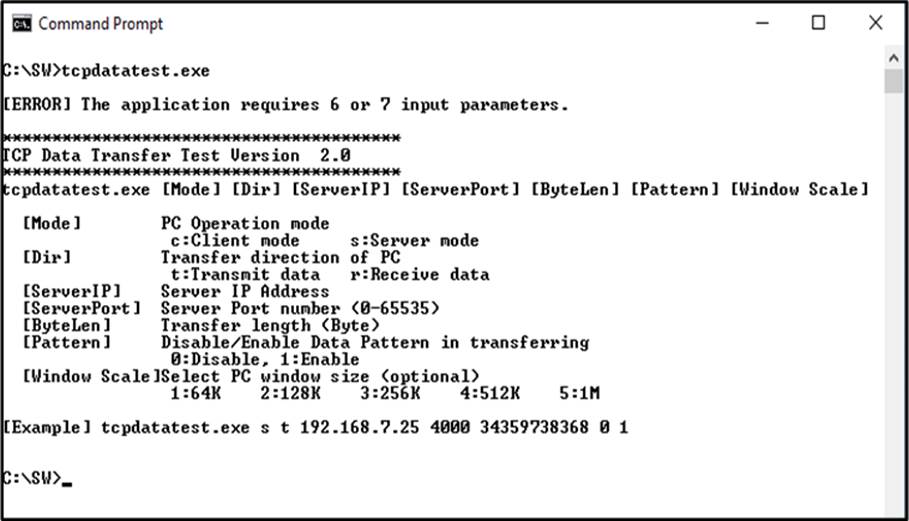
Figure 4‑1 �tcpdatatest� Application Usage
The �tcpdatatest� application is used to send or receive TCP data on a PC. It requires six mandatory parameters and one optional parameter. Ensure that the parameter inputs match those configured on the FPGA. The details for each parameter are outlined below.
Mandatory Parameters
1) Mode : c � The PC runs in Client mode while the FPGA runs in Server mode
s � The PC runs in Server mode while the FPGA runs in Client mode
2) Dir : t � Transmit mode (the PC sends data to the FPGA)
r � Receive mode (the PC receives data from the FPGA)
3) ServerIP : The IP address of the FPGA when the PC runs in Client mode
(Default is 192.168.7.42).
4) ServerPort : The port number of the FPGA when the PC runs in Client mode
(Default is 60000).
5) ByteLen : The total size of data to be transferred in bytes. This parameter is used
only in Transmit mode and is ignored in Receive mode. In Transmit
mode, the �ByteLen� value must match the total transfer size set in the
�Receive data test� menu on the FPGA. In Receive mode, the
application terminates once the connection is closed.
6) Pattern : 0 � Generate dummy data in Transmit mode and disable data
verification in Receive mode.
1 � Generate incremental data in Transmit mode and enable data
verification in Receive mode.
Optional parameter
1) Window Scale : Indicate the size of the allocated buffer for the TCP socket on the PC
and control the TCP Window scaling feature. The valid range is 1-5.
1 � Allocated buffer size of 64 KB
2 � Allocated buffer size of 128 KB
3 � Allocated buffer size of 256 KB
4 � Allocated buffer size of 512 KB
5 � Allocated buffer size of 1 MB
The sequence of the test application when running in Transmit mode and Receive mode are detailed below.
1) Obtain and validate the user�s input parameters, excluding the optional Window Scale parameter.
2) Create a socket, configure the socket options, and specify the socket memory size.
3) Establish a new connection using the provided Server IP address and Server port number.
4) Allocate 2 MB of memory for the send buffer.
5) If the dummy data is not selected, generate an incremental test pattern to the send buffer.
6) Send the data through the socket and keep track of the total amount of data sent.
7) Calculate the remaining data size to be transferred.
8) Display the total amount of data transferred every second.
9) Repeat step 5) � 8) until all the data has been transferred (the remaining transfer size reaches 0).
10) Calculate the overall performance and display the result on the console.
11) Close the socket and free the allocated memory.
Receive mode
1) Follow the step 1) � 3) of the Transmit mode sequence.
2) Allocate 2 MB of memory for the receive buffer.
3) Continuously wait for data to be stored in the receive buffer, read it, and update the total amount of received data.
4) If data verification is enabled, compare the received data with the incremental pattern. Print an error message if a mismatch is detected. If verification is disabled, skip this step.
5) Display the total amount of received data every second.
6) Repeat steps 3) � 5) until the connection is closed by the transmitting device.
7) Calculate the overall performance and display the result on the console.
8) Close the socket and free the allocated memory.
4.2 �tcp_client_txrx_xg� for Full Duplex Test
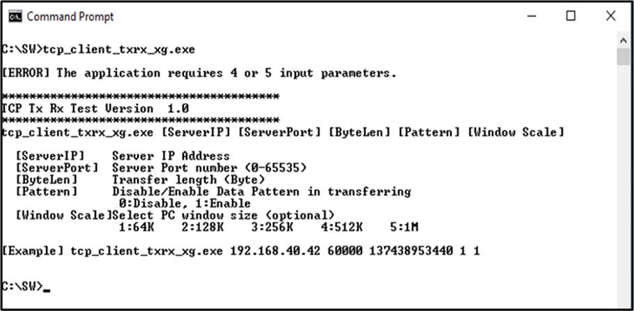
Figure 4‑2 �tcp_client_txrx_xg� Application Usage
The �tcp_client_txrx_xg� application allows the PC to simultaneously send and receive TCP data over Ethernet using the same port number. This application runs exclusively in Client mode and requires Server parameters (the network parameters of TOE10G-IP) to be input by the user. The application uses five parameters, outlined below.
Mandatory parameters
1) ServerIP : The IP address of the FPGA
2) ServerPort : The port number of FPGA
3) ByteLen : The total transfer size in bytes, representing the total amount of
transmitted and received data. This value must match the transfer size
set on the FPGA for the full duplex test.
4) Pattern : 0 � Generate dummy data for the sending function and disable data
verification for the receiving function. This mode is used to measure the
maximum performance of full-duplex transfer.
1 � Generate incremental data for the sending function and enable data
verification for the receiving function.
Optional parameter
1) Window Scale : Indicate the size of the allocated buffer for the TCP socket on the PC
and control the TCP Window scaling feature. The valid range is 1-5.
1 � Allocated buffer size of 64 KB
2 � Allocated buffer size of 128 KB
3 � Allocated buffer size of 256 KB
4 � Allocated buffer size of 512 KB
5 � Allocated buffer size of 1 MB
Note: The Window Scale parameter is optional. If the user does not provide this parameter, it is automatically set to 1. The default TOE10G-IP does not have Window Scale features enabled. If you require the use of this feature, please contact our sales team for assistance.
The sequence of the test application when running the application is detailed below.
1) Obtain and verify the user�s input parameters, excluding the optional Window Scale parameter.
2) Allocate 2 MB of memory separately for the send and receive buffers.
3) Create a socket, configure the socket options, and specify the socket memory size.
4) Establish a new connection using the provided Server IP address and Server port number.
5) If the dummy data is not selected, generate an incremental test pattern to the send buffer.
6) If the send function is not ready for operating, skip this step; otherwise, continue the following steps.
i) If the test pattern is enabled, generate the incremental test pattern in the send buffer; otherwise, skip this step for dummy data.
ii) Send the data through the socket and keep track of the total amount of data sent.
iii) Calculate the remaining data size to be transmitted.
7) If the receive function is not ready for operating, skip this step; otherwise, continue the following steps.
i) Read the data from the receive buffer and update the total amount of received data.
ii) If the test pattern is enabled, verify the received data using the incremental pattern, and print an error message if verification fails; otherwise, skip this step.
8) Display the total amount of transmitted and received data every second.
9) Repeat steps 5) � 8) until the total amount of transmitted and received data equals �ByteLen� value set by the user.
10) Calculate the performance and print the result on the console.
11) Close the socket.
12) Pause for 1 second to allow the hardware to complete the current test loop.
13) Start a new test by repeating steps 3) � 12) in forever loop. However, if the data verification fails at any point, terminate the application.
5 Revision History
|
Revision |
Date (D/M/Y) |
Description |
|
2.00 |
4-Sep-24 |
- Support Fixed-MAC mode. - Change full-duplex test application to �tcp_client_txrx_xg�. - Update USER_FFSTS_INTREG register in [19:6] following the update of TCPRxFfRdCnt. - Add USER_INT_INTREG to register map and update firmware to use Connection status interrupt. - Support MRMAC IP Core for Versal device |
|
1.05 |
15-Mar-22 |
Update reverse packet feature |
|
1.04 |
24-Aug-20 |
Rename IP from TenGEMAC to 10G25EMAC |
|
1.03 |
22-Jul-20 |
Update register in the firmware |
|
1.02 |
22-Aug-19 |
Add function list and use tcp_client_txrx_40G software |
|
1.01 |
2-Apr-18 |
Support FPGA<->FPGA connection |
|
1.00 |
22-Jan-18 |
Initial version release |