UDP1G-IP Core Data Sheet

Core Facts |
|
|
Provided with Core |
|
|
Documentation |
User Guide, Design Guide |
|
Design File Formats |
Encrypted hdl File |
|
Verification |
Test Bench, Simulation Library |
|
Instantiation Templates |
VHDL |
|
Reference Designs & Application Notes |
QuartusII Project, See Reference Design Manual |
|
Additional Items |
Demo on CycloneV E/ArriaV GX/ Cyclone10 GX/Arria10 SoC/ Arria10 GX Development Board |
|
Support |
|
|
Support Provided by Design Gateway Co., Ltd. |
|
Design Gateway Co.,Ltd
E-mail: ip-sales@design-gateway.com
URL: www.design-gateway.com
Features
· UDP/IP stack implementation
· Support IPv4 protocol
· Full-duplex transferring by using two port numbers for each transfer direction
· Support more sessions by using multiple UDP1G-IPs
· Various Transmit/Receive buffer size (2 KB, 4KB, 8KB, 16KB, 32KB, and 64KB)
· Simple data interface by standard FIFO interface
· Simple control interface by single port RAM interface
· 8-bit Avalon stream to interface with Triple-Speed Ethernet MAC from Intel
· User clock frequency fixed to 125 MHz clock frequency
· Reference design available on CycloneVE/ArriaV GX/Cyclone10GX/Arria10 SoC/Arria10 GX Development Board
· Support IP fragmentation
· Customized service for following features
· Multicast IP
· Network parameter assignment by other methods
Table 1: Example Implementation Statistics
|
Family |
Example Device |
Fmax (MHz) |
ALMs |
Registers1 |
Pin |
Block Memory bit2 |
Design Tools |
|
CycloneV E |
5CEFA7F31I7 |
125 |
1,030 |
1,628 |
- |
1,181,696 |
QuartusII 16.0 |
|
ArriaV GX |
5AGXFB3H4F35C5 |
125 |
1,028 |
1,608 |
- |
1,181,696 |
QuartusII 16.0 |
|
Cyclone10 GX |
10GX220YF780E5G |
125 |
1,001 |
1,685 |
- |
1,181,696 |
QuartusII 18.0 |
|
Arria10 SX |
10AS066N3F40E2SGE2 |
125 |
1,032 |
1,702 |
- |
1,181,696 |
QuartusII 16.0 |
Notes:
1) Actual logic resource dependent on percentage of unrelated logic
2) Block memory resources are based on 64k Tx data buffer size, 16k Tx packet buffer size, and 64k Rx data buffer size.
Applications
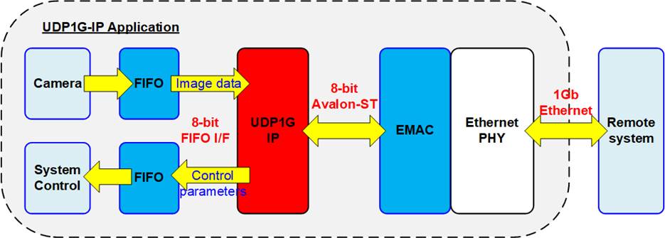
Figure 1: UDP1G IP Application
1 Gb Ethernet is the well-known communication channel for transferring data with remote controlling system. By using UDP/IP protocol for data streaming via 1Gb Ethernet, the system can transfer data stream at high speed rate. UDP1G IP is the IP which is integrated to the system for transfering data via 1 Gb Ethernet without using CPU and external memory. So, the IP can fit with the application which needs to send and receive data at high-speed rate based on FPGA solution such as video data streaming from camera and the monitoring system.
Figure 1 shows the example application of video camera system. The video data from camera is streaming to the FIFO and then forwarded to remote system via 1 Gb Ethernet by UDP1G IP. UDP1G IP is desigend to support bi-directional transfer at the same time by using different port numbers, so Remote system can send the updated parameters for real-time controlling the system via 1 Gb Ethernet.
General Description
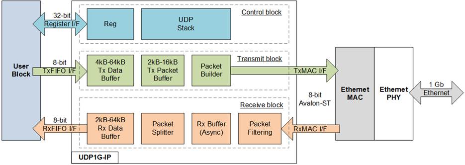
Figure 2: UDP1G-IP Block Diagram
UDP1G IP core implements UDP/IP stack by hardware logic and connects with EMAC IP and external PHY module as the lower layer hardware. User interface of UDP1G IP consists of two interfaces - Register interface for control signals and FIFO interface for data signals.
Register interface has 4-bit address for accessing up to 16 registers, consisting of network parameters, command register, and system parameters. The IP uses two sessions for transferring data in bi-directional, one session for one direction. All network parameters of both sessions must be similar, except the port number on the target device. The network parameters are assigned by the user to be fixed value for both UDP1G IP and the target device before starting IP initialization. The reset process is necessary when some network parameters must be changed. The initialization process has two modes to get MAC address of the target device. After finishing the initialization process, the IP is ready for transferring data with the target device.
To send the data, the user sets total transfer size and packet size to the IP and then transfers the data via TxFIFO interface which is 8-bit data size. When the data is received from the target, the user reads the received data from the IP via RxFIFO interface.
To meet the user system requirement which may be sensitive on the memory resource or the performance, the buffer size inside the IP can be assigned by the user. In Tx path, two buffers can be adjusted - Tx data buffer and Tx packet buffer. In Rx path, one buffer is available, named Rx data buffer. Buffer size in the IP is applied to be the data buffer between user logic and EMAC. By using bigger buffer size, the user logic can switch to run other tasks for longer time before switching back to transfer the data with UDP1G IP.
Functional Description
Control Block
· Reg
All parameters of the IP are set via register interface which uses 4-bit address and 32-bit data bus. Timing diagram of register interface is similar to single-port RAM interface. The address is shared for both write and read directions.The description of each register is defined as shown in Table 2.
Table 2: Register map Definition
|
RegAddr [3:0] |
Reg Name |
Dir |
Bit |
Description |
|
0000b |
RST |
Wr/ Rd |
[0] |
Reset IP. �0�: No reset, �1�: Reset. Default value is �1�. After all parameters are assigned, the user sets �0� to this register for loading parameters and start system initialization. User must set this register to �1� and �0� respectively when some network paramters are changed. The network parameters controlled by RST register are SML, SMH, DIP, SIP, DPN, SPN, and SRV register. |
|
0001b |
CMD |
Wr |
[0] |
User command. Set �1� to start sending data. Before setting this register to start new operation, user needs to confirm that the system is in Idle status by checking busy signal de-asserted to �0�. Busy signal is the IP output and can be read by bit[0] of CMD register. |
|
Rd |
[0] |
System busy flag. �0�: Idle, �1�: IP is busy from initialization or send command. This signal is also mapped as Busy (IP output signal). |
||
|
0010b |
SML |
Wr/ Rd |
[31:0] |
Define 32-bit lower MAC address (bit [31:0]) for this IP. To update this value, the IP must be reset by RST register. |
|
0011b |
SMH |
Wr/ Rd |
[15:0] |
Define 16-bit upper MAC address (bit [47:32]) for this IP. To update this value, the IP must be reset by RST register. |
|
0100b |
DIP |
Wr/ Rd |
[31:0] |
Define 32-bit target IP address. To update this value, the IP must be reset by RST register. |
|
0101b |
SIP |
Wr/ Rd |
[31:0] |
Define 32-bit IP address for this IP. To update this value, the IP must be reset by RST register. |
|
0110b |
DPN |
Wr /Rd |
[31:0] |
[15:0]-Define 16-bit target port number for IP sending data. [31:16]-Define 16-bit target port number for IP receiving data. To update this value, the IP must be reset by RST register. |
|
0111b |
SPN |
Wr /Rd |
[15:0] |
Define 16-bit port number for this IP. To update this value, the IP must be reset by RST register. |
|
1000b |
TDL |
Wr |
[31:0] |
Total Tx data length in byte unit. Valid range is 1-0xFFFFFFFF. User needs to set this register before setting CMD register=�1�. The IP loads TDL register when CMD register is set. After the IP runs Send data command (Busy=�1�), the user can set the new value of TDL register for the next command. The user does not need to set TDL register again when the next command uses the same total data length. |
|
Rd |
Remaining transfer length in byte unit which does not transmit. |
|
RegAddr [3:0] |
Reg Name |
Dir |
Bit |
Description |
|
1001b |
TMO |
Wr |
[31:0] |
Define timeout value for waiting ARP reply packet after sending ARP request. The counter is run under 125 MHz, so timer unit is equal to 8 ns. IntOut is asserted to �1� when the ARP reply is not received in time. This value is recommended to be more than 0x6000. |
|
Rd |
The details of timeout interrupt. [0]-Timeout from not receiving ARP reply packet After timeout, IP resends ARP request until ARP reply is received. [8]-Rx packet ignored because of Rx data buffer full [9]-Rx packet ignored because of checksum failed [10]-Rx packet ignored because of MacRxError error |
|||
|
1010b |
PKL |
Wr /Rd |
[15:0] |
UDP data length of one Tx packet in byte unit. Valid from 1-16000. Default value is 1472 byte which is the maximum size for non-jumbo frame. During running Send data command (Busy=�1�), the user must not set this register. Similar to TDL register, the user does not need to set PKL register again when the next command uses the same packet length. |
|
1110b |
SRV |
Wr/ Rd |
[0] |
�0�: Client mode (default). After RST register changes from �1� to �0�, the IP sends ARP request to get Target MAC address from the ARP reply returned by the target device. IP busy is deasserted to �0� after receiving ARP reply. �1�: Server mode. After RST register changes from �1� to �0�, the IP waits ARP request from the Target to get Target MAC address. After receiving ARP request, the IP generates ARP reply and then de-asserts IP busy to �0�. Note: In Server mode, when RST register changes from �1� to �0�, the target device needs to resend ARP request for UDP1G IP completing the IP initialization. |
|
1111b |
VER |
Rd |
[31:0] |
IP version |
· UDP Stack
UDP stack is the main controller of the IP for controlling the other modules in every process. The IP operation has two phases - IP initialization phase and data transferring phase.
After RST register changes from �1� to �0�, the initialization phase begins. There are two modes for running the initialization phase, set by SRV[0] register, i.e., Client mode and Server mode. The parameters from Reg module are read by UDP Stack and then set to Transmit block and Receive block for transferring the packet to complete the initialization process, following the mode. After that, the IP changes to data transferring phase.
UDP1G IP supports full-duplex transfer, so UDP1G IP can send data to the target device and receive data from the target device at the same time. Busy signal is asserted to �1� during sending data and de-asserted to �0� after finishing sending data.
To send the data, the data from the user is stored in Tx data buffer and Tx packet buffer. After the network parameters are read to build UDP header by Packet Builder, Transmit block sends UDP packet including the data from the user to the target device via Ethernet MAC.
When the data is received by Receive block, Busy signal is not asserted. UDP Stack is ready for running Send command. Therefore, full-duplex transfer can be run with full performance.
Table 3: TxBuf/TxPac/RxBufBitWidth Parameter description
|
Value of BitWidth |
Buffer Size |
TxBufBitWidth |
TxPacBitWidth |
RxBufBitWidth |
|
11 |
2kByte |
No |
Valid |
Valid |
|
12 |
4kByte |
Valid |
Valid |
Valid |
|
13 |
8kByte |
Valid |
Valid |
Valid |
|
14 |
16kByte |
Valid |
Valid |
Valid |
|
15 |
32kByte |
Valid |
No |
Valid |
|
16 |
64kByte |
Valid |
No |
Valid |
Transmit Block
There are two buffers in Transmit block - Tx data buffer and Tx packet buffer which the size can be adjusted by parameter assignment. The minimum size of Tx data buffer and Tx packet buffer is limited by the transmit packet size, set by PKL register. Data from Tx data buffer is split to one packet size and stored in Tx packet buffer. UDP header is prepared and then combined with UDP data from Tx packet buffer to build complete UDP packet. The data in Tx data buffer can be flushed after the data is forwarded to EMAC. After finishing the send data command, the user can change the packet size and total data size for the new send data command by updating PKL and TDL register respectively.
· Tx Data Buffer
This buffer size is set by �TxBufBitWidth� parameter of the IP. The valid value is 12-16 which is equal to the address size of buffer, as shown in Table 3. The buffer size should be more than or equal to two times of Tx Packet Size, set by PKL register. If Tx data buffer always stores at least two packet data, UDP1G IP can transfer data to EMAC continuously and the system can get the best transmit performance on 1Gb Ethernet. Also, this buffer is the data buffer for the user logic. Using the bigger size allows the user logic to have longer time for switching to run other tasks before going back to handle with the data interface of Tx data buffer.
· Tx Packet Buffer
The size is set by �TxPacBitWidth� parameter of the IP. The valid value is 11-14 and the description of the parameter is shown in Table 3. This buffer size must be more than Tx Packet size + 4. For example, when TxPacBitWidth=11, maximum value for PKL is 2044 (2048-4). At most, two packets are stored in Tx Packet buffer. The user select the size of Tx packet buffer to fit with the user�s system requirement.
· Packet Builder
UDP packet consists of the header and the data. Packet builder receives network parameters, set in Reg module, and then prepares UDP header. Also, IP and UDP checksum are calculated to be UDP header. After that, all UDP header is built, the header combining with the data from Tx packet buffer is transmitted to EMAC.
Receive Block
· Rx Buffer
This is temporary buffer to store the received packets from EMAC when the previous packet is not completely processed. Also, the buffer is designed as asynchronous buffer to convert clock domain of received data stream from receive clock to be transmit clock.
· Packet Filtering
The header in Rx packet are verifed by this module to validate the packet. The packet is valid when the following conditions are met.
(1) Network parameters are matched to the value in Reg module, i.e., MAC address, IP address, and Port number.
(2) The packet is ARP packet or UDP/IPv4 packet.
(3) IP header length is valid (IP header length is equal to 20 bytes).
(4) IP data length and UDP data length must be matched.
(5) IP checksum and UDP checksum are correct or disabled.
Note: UDP checksum is not verified for fragment packet.
(6) In case of fragment packet, the packet must be received in a good sequence, not swapped.
· Packet Splitter
This module is designed to remove the packet header and split only UDP data to store to Rx data buffer.
· Rx Data Buffer
This buffer size is set by �RxBufBitWidth� parameter of the IP. The valid value is 11-16 for 2Kbyte � 64Kbyte buffer size. This is the data buffer between user logic and UDP1G IP for receiving data operation. If user logic does not read data from Rx data buffer for long time until the buffer is full, the new received packet will be ignored. The minimum size of Rx data buffer is recommended to be equal to two times of receive packet size or more. Bigger buffer size can store more data when the user logic is not available to read data from UDP1G IP. The proper size depends on the unavailable time of the user logic for reading the data.
User Block
This module can be designed by using state machine to set the command and the parameters via register interface. Also, the status can be monitored to confirm the operation is finished without any error. The data path can connect with the FIFO for sending or receiving data with the IP.
Ethernet MAC
The reference design of the IP uses tri-speed Ethernet MAC from Intel FPGA. UDP1G IP can directly connect to Intel FPGA EMAC IP. More details of the IP are provided in following website.
Core I/O Signals
Descriptions of all parameters and signal I/O are provided in Table 4 - Table 7. The EMAC interface is designed to connect with Intel EMAC following Avalon stream standard.
Table 4: Core Parameters
|
Generic Name |
Value |
Description |
|
TxBufBitWidth |
12-16 |
Setting Tx Data buffer size. The value is referred to address bus size of this buffer. |
|
TxPacBitWidth |
11-14 |
Setting Tx Packet buffer size. The value is referred to address bus size of this buffer. |
|
RxBufBitWidth |
11-16 |
Setting Rx Data buffer size. The value is referred to address bus size of this buffer. |
Table 5: Core I/O Signals (Synchronous with Clk)
|
Signal |
Dir |
Description |
|
Common Interface Signal |
||
|
RstB |
In |
Reset IP core. Active Low. |
|
Clk |
In |
125 MHz fixed clock frequency to synchronous with transmit interface of 1Gb EMAC. |
|
User Interface |
||
|
RegAddr[3:0] |
In |
Register address bus. In Write access, RegAddr is valid when RegWrEn=�1�. |
|
RegWrData[31:0] |
In |
Register write data bus. Valid when RegWrEn=�1�. |
|
RegWrEn |
In |
Register write enable. Valid at the same clock as RegAddr and RegWrData. |
|
RegRdData[31:0] |
Out |
Register read data bus. Valid in the next clock after RegAddr is valid. |
|
Busy |
Out |
IP busy status (�0�-Idle, �1�-IP is busy from initialization or sending data). This signal is mapped to bit0 of CMD register. |
|
IntOut |
Out |
Assert to high for 1 clock cycle when timeout is detected or Rx packet is ignored. More details of Interrupt status could be checked from TMO[10:0] register. |
|
Tx Data Buffer Interface |
||
|
UDPTxFfFull |
Out |
Asserted to �1� when Tx data buffer is full. User needs to stop writing data within 4 clock cycles after this flag is asserted to �1�. |
|
UDPTxFfWrEn |
In |
Write enable to Tx data buffer. Asserted to �1� to write data to Tx data buffer. |
|
UDPTxFfWrData[7:0] |
In |
Write data to Tx data buffer. Valid when UDPTxFfWrEn=�1�. |
|
Rx Data Buffer Interface |
||
|
UDPRxFfRdCnt[15:0] |
Out |
Data counter of Rx data buffer to show the number of received data in byte unit. |
|
UDPRxFfRdEmpty |
Out |
Asserted to �1� when Rx data buffer is empty. User needs to stop reading data immediately when this signal is asserted to �1�. |
|
UDPRxFfRdEn |
In |
Assert to �1� to read data from Rx data buffer. |
|
UDPRxFfRdData[7:0] |
Out |
Data output from Rx data buffer. Valid in the next clock cycle after UDPRxFfRdEn is asserted to �1�. |
Table 6: Tx EMAC Interface (Synchronous with Clk)
|
Signal |
Dir |
Description |
|
Transmit MAC Interface |
||
|
MacTxData[7:0] |
Out |
Transmitted data. Valid when MacTxValid=�1�. |
|
MacTxValid |
Out |
Valid signal of transmitted data. This signal is asserted to �1� to send one frame continuously. |
|
MacTxSOP |
Out |
Control signal to indicate the first word in the frame. Valid when MacTxValid=�1�. |
|
MacTxEOP |
Out |
Control signal to indicate the final word in the frame. Valid when MacTxValid=�1�. |
|
MacTxReady |
In |
Handshaking signal. Asserted to �1� when MacTxData has been accepted. This signal must not be de-asserted to �0� when a packet is transmitting. |
Table 7: Rx EMAC Interface (Synchronous with MacRxClk)
|
Signal |
Dir |
Description |
|
Receive MAC Interface |
||
|
MacRxClk |
In |
Receive clock from EMAC for synchronous with Receive interface |
|
MacRxData[7:0] |
In |
Received data. Valid when MacRxValid=�1�. |
|
MacRxValid |
In |
Valid signal of received data. MacRxValid must be asserted to �1� continuously for transferring a packet. |
|
MacRxSOP |
In |
Control signal to indicate the first word in the frame. Valid when MacRxValid=�1�. |
|
MacRxEOP |
In |
Control signal to indicate the final word in the frame. Valid when MacRxValid=�1�. |
|
MacRxError |
In |
Control signal asserted at the end of received frame (MacRxValid=�1� and MacRxEOP=�1�) to indicate that the frame has CRC error. �1�: error packet, �0�: normal packet. |
|
MacRxReady |
Out |
Handshaking signal. Asserted to �1� when MacRxData has been accepted. MacRxReady is de-asserted to �0� for 3 clock cycles to be the gap size between each received packet. |
Timing Diagram
IP Initialization
The initialization process begins after user changes RST register from �1� to �0�. UDP1G IP can run in two modes, set by SRV[0] register, i.e., Client mode (SRV[0]=�0�) and Server mode (SRV[0]=�1�). The details of each mode are shown in the following timing diagram.
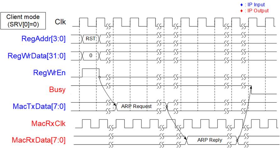
Figure 3: IP Initialization in Client mode
As shown in Figure 3, in Client mode UDP1G IP sends ARP request and waits for ARP reply returned from the target device. Target MAC address is extracted from ARP reply packet. After finishing, Busy signal is de-asserted to �0�.
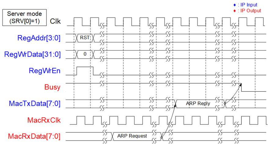
Figure 4: IP Initialization in Server mode
As shown in Figure 4, after reset process in Server mode, UDP1G IP waits for ARP request sent by the target device. After that, UDP1G IP returns ARP reply to the target. Target MAC address is extracted from ARP request packet. Finally, Busy signal is de-asserted to �0�.
Register Interface
As shown in Figure 5, to write the register, the user sets RegWrEn=�1� with the valid value of RegAddr and RegWrData. To read the register, the user sets only RegAddr and then RegRdData is valid in the next clock cycle.

Figure 5: Register interface timing diagram
As shown in Figure 6, before the user sets CMD register to start the new command operation, Busy flag must be equal to �0� to confirm that IP is in Idle status. After CMD register is set, Busy flag is asserted to �1�. Busy is de-asserted to �0� when the command is completed.
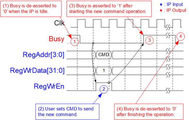
Figure 6: CMD register timing diagram
Tx FIFO Interface
To send the data to IP core via Tx FIFO interface, Full flag is monitored to be flow control signal. The write signals are similar to write interface of general FIFO by using write data and write enable as shown in as shown in Figure 7.
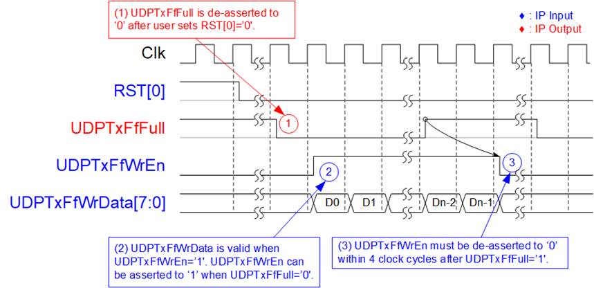
Figure 7: Tx FIFO interface timing diagram
(1) During IP is in reset condition, UDPTxFfFull is asserted to �1� and all data in FIFO are flushed.
(2) Before sending data, user needs to confirm that full flag (UDPTxFfFull) is not asserted to �1�. After that, UDPTxFfWrEn can be asserted to �1� with valid value of UDPTxFfWrData.
(3) UDPTxFfWrEn must be de-asserted to �0� within 4 clock cycles to pause data sending after UDPTxFfFull is asserted to �1�.
Note: Data in Tx FIFO is not lost or flushed until the IP is reset.
Rx FIFO Interface
After the received data is stored in Rx data buffer, the user can read the data from Rx data buffer by using Rx FIFO interface. Empty flag is monitored to check data available status and then asserts read enable signal to read the data, similar to read interface of general FIFO, as shown in Figure 8.
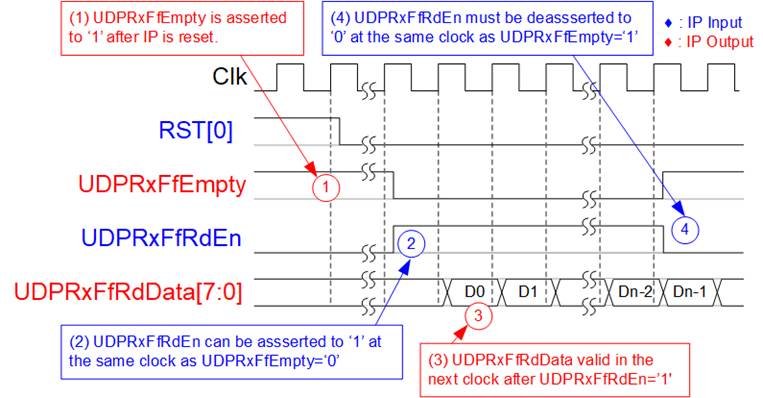
Figure 8: Rx FIFO interface timing diagram by Empty flag
(1) After the IP finishes reset process, there is no data in Rx data buffer (UDPRxFfEmpty=�1�).
(2) UDPRxFfEmpty is monitored to check data available status. When data is ready (UDPRxFfEmpty =�0�), UDPRxFfRdEn can be asserted to �1� to read data from Rx data buffer.
(3) UDPRxFfRdData is valid in the next clock cycle.
(4) Reading data must be immediately paused by de-asserting UDPRxFfRdEn=�0� when UDPRxFfEmpty =�1�.
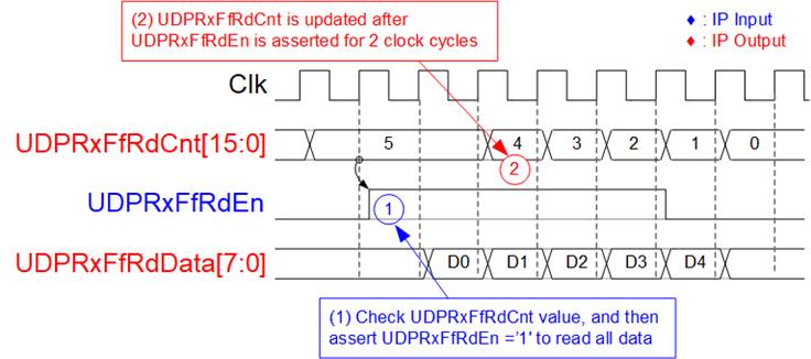
Figure 9: Rx FIFO interface timing diagram by using read counter
If user logic reads data as burst mode, UDP1G IP has read counter signal to show the total data stored in Rx FIFO interface as byte unit. For example in Figure 9, there are five data available in Rx data buffer. So, user can assert UDPRxFfRdEn to �1� for 5 clock cycles to read all data from Rx data buffer. The latency time between read counter (UDPRxFfRdCnt) and read enable (UDPRxFfRdEn) is 2 clock cycles.
EMAC Interface
EMAC interface of UDP1G IP is designed by using 8-bit Avalon-stream interface. The limitation is that UDP1G IP cannot pause data transmission when the packet does not end. So, MacTxReady must be asserted to �1� during transmitting a packet. MacTxReady can be de-asserted to �0� after the last data in the packet is transferred, as shown in Figure 10.
Figure 10: Transmit EMAC Interface
(1) UDP1G IP asserts MacTxSOP and MacTxValid to �1� with the first data of the packet. All signals are latched until MacTxReady is asserted to �1� to accept the first data.
(2) After the first data is accepted, MacTxReady must be asserted to �1� to accept all remaining data in the packet from UDP1G IP until end of packet. The IP sends all data of one packet continuously.
(3) MacTxEOP and MacTxValid are asserted to �1� when the last data of the packet is transmitted.
(4) After the end of packet, MacTxReady can be asserted to �0� to pause the next packet transmission.
(5)
Similar to Transmit EMAC interface, the data of one packet must be received continuously in Receive EMAC interface. Valid signal must be asserted to �1� from the start of the packet to the end of the packet. Timing diagram of Receive EMAC interface has two formats. First is timing diagram when connecting with Intel EMAC IP, as shown in Figure 11. Second is timing diagram when connecting with other modules by using Avalon-ST interface, as shown in Figure 12.
UDP1G IP needs to run post processing after finishing each received packet, so it needs to have 3-clock cycle gap size between each packet transmission. Intel EMAC IP always de-asserts valid signal to pause data transmission in Receive EMAC interface for 3 clock cycles before asserting end-of-packet. So, MacRxReady, output from UDP1G IP, is always asserted to �1� when connecting with Intel EMAC IP.
Figure 11: Receive EMAC Interface when connecting with Intel EMAC
(1) UDP1G IP detects the start of received frame when MacRxSOP and MacRxValid are asserted to �1�. At the same time, the 1st received data is read from MacRxData to start packet processing by UDP1G IP. MacRxReady is always asserted to �1� until end of the packet.
(2) The last data must be valid on MacRxData for UDP1G IP reading although the control signal to show the last data still not be transmitted from EMAC. UDP1G IP needs to read data of one packet continuously.
(3) EMAC de-asserts MacRxValid for 3 clock cycles to receive and validate 32-bit CRC of Ethernet packet.
(4) MacRxEOP and MacRxValid are asserted to �1� to send the end of packet. UDP1G IP reads MacRxError to validate if the packet has the good CRC status. The IP ignores the packet when MacRxError is asserted.
Some user applications does not connect UDP1G IP to Intel EMAC, but connecting to other modules through Avalon-ST bus. MacRxValid is asserted to �1� continuously until end of packet. In this case, MacRxReady is de-asserted to �0� for 3 clock cycles to pause the next packet, as shown in Figure 12.
Figure 12: Receive EMAC Interface when connecting through other modules
(1) UDP1G IP detects start of the received frame when MacRxSOP=�1� and MacRxValid=�1�. In this cycle, the first data is valid on MacRxData. After that, MacRxReady is asserted to �1� to accept all data until the end of the packet. In this condition, MacRxValid is asserted to �1� for transmitting the data of one packet continuously.
(2) The end of the packet is detected when MacRxEOP=�1� and MacRxValid=�1�. At the same clock, the last data is valid on MacRxData.
(3) After that, UDP1G IP de-asserts MacRxReady for 3 clock cycles to complete the packet post processing.
Example usage
Client mode (SRV[0]=�0�)
The example sequence to set register for transferring data in Client mode is shown as follows.
1) Set RST register=�1� to reset the IP.
2) Set SML/SMH for MAC address, DIP/SIP for IP address, and DPN/SPN for port number.
3) Set RST register=�0� to start the IP initialization process by sending ARP request packet to get Target MAC address from ARP reply packet. Busy signal is de-asserted to �0� after finishing the initialization process.
4) a. For data transmission, set TDL register (total transmit length) and PKL register (packet size). Next, set CMD register = �1� to start data transmission. The user sends the data to UDP1G IP via TxFIFO interface before or after setting CMD register. When the command is finished, busy flag changes to �0�. The user can set the new value to TDL/PKL register and then set CMD register = �1� to start the next transmission.
b. For data reception, user monitors RxFIFO status and reads data until RxFIFO is empty.
Server mode (SRV[0]=�1�)
Comparing to Client mode which MAC address is decoded from ARP reply packet after UDP1G IP sends ARP request packet, Server mode decodes MAC address from ARP request packet. The process for transferring data is the same as Client mode. The example step of Server mode is shown as follows.
1) Set RST register=�1� to reset the IP.
2) Set SML/SMH for MAC address, DIP/SIP for IP address, and DPN/SPN for port number.
3) Set RST register=�0� to start the IP initialization process by waiting ARP request packet to get Target MAC address. Next, the IP creates ARP reply packet returned to the target device. After finishing the intialization, busy signal is de-asserted to �0�.
4) Remaining steps are similar to step 4 of Client mode.
Verification Methods
The UDP1G-IP Core functionality was verified by simulation and also proved on real board design by using CycloneV E/ArriaV GX/Cyclone10 GX/Arria10 SoC/Arria10 GX development board.
Recommended Design Experience
User must be familiar with HDL design methodology to integrate this IP into system.
Ordering Information
This product is available directly from Design Gateway Co., Ltd. Please contact Design Gateway Co., Ltd. For pricing and additional information about this product using the contact information on the front page of this datasheet.
Revision History
|
Revision |
Date |
Description |
|
1.0 |
27-Feb-2017 |
New release |
|
1.1 |
1-Mar-2017 |
Update Figure11 |
|
1.2 |
10-Aug-2018 |
Add SRV register and MacRxReady |
|
1.3 |
26-Nov-2019 |
Support Cyclone10GX device |
|
1.4 |
2-Oct-2020 |
Update company info |
|
1.5 |
26-Mar-2021 |
Support Arria10GX device |