![]() U.2-PCIe
adapter board [AB20-U2PCI] Manual [ Rev. 1.0E]
U.2-PCIe
adapter board [AB20-U2PCI] Manual [ Rev. 1.0E]
Introduction
Thank you for choosing U.2 – PCIe conversion adapter board [Part Number: AB20-U2PCI] ( gadapter board h in this manual). This adapter board converts 16-lane PCI Express interface to four 4-lane PCI standard U.2 interfaces. This adapter can be applied to standard altera(Intel) or AMD(Xilinx) FPGA evaluation board so that user can evaluate NVMe series IP-Core operation and can use for prototype development platform.
Four U.2 connectors are mounted on the component side of the adapter board to accommodate up to four 2.5 h form factor U.2 SSDs. On the solder side, 16-lane PCIe (PCI Express) connector is mounted, and lanes 3-0/7-4/11-8/15-12 connect to four SSDs mounted on CN1/CN2/CN3/CN4, respectively.
The adapter includes a low-jitter clock generator and reset circuitry to provide clock and reset signals to PCIe and U.2 SSDs. Power for the adapter and U.2 SSDs is provided by a standard 6-pin type PCI Express auxiliary power supply.
The adapter board furnishes mechanical support frame to mount U.2 SSD in stable position.
The adapter with support frame together with U.2 SSD and FPGA board is shown in Figure 1 below.
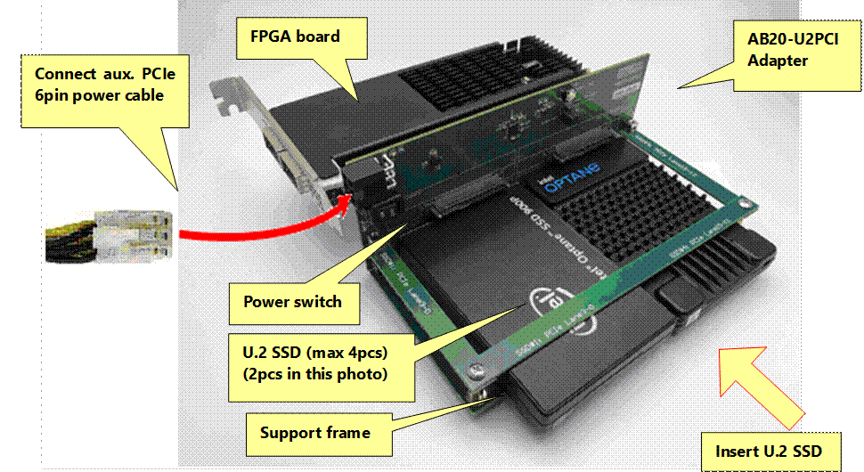
Figure-1: AB20-U2PCI
adapter with support frame
The features of this adapter are shown below.
ü Expansion adapter board for U.2 SSD with 16-Lane PCI Express support
ü Read/write access between FPGA and U.2 SSD in PCIe Gen5, confirmed in actual device operation
ü Up to four U.2 SSDs under 15mm height size can be installed simultaneously
ü Power is supplied at +12V from a standard external 6-pin PCIe auxiliary power supply
ü Power supply to the adapter and U.2 SSD can be controlled ON/OFF with a switch
ü PCIe standard 100MHz low-jitter clock source mounted on the adapter
ü Supplies 100MHz differential clock signals of the same phase to PCIe and four SSDs
ü Reset is selectable between PCIe-SSD direct connection and reset output on the adapter board via jumper socket
Adapter outline
The adapter board with support frame size is 166 mm wide, 60mm height, and 85mm depth. @The component side and the solder side of the board are shown in Figure 2 and Figure 3 respectively.
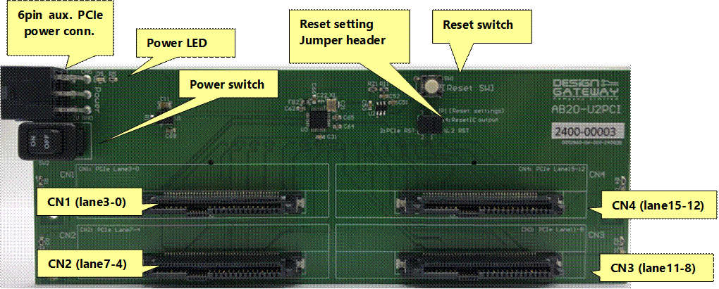
Figure-2: adapter
board component side
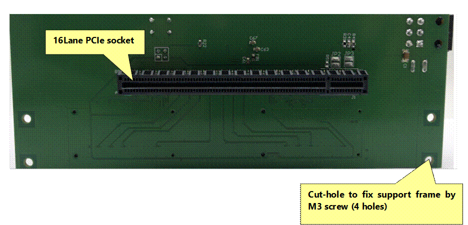
Figure-3: adapter board solder side
Power Supply
This adapter power is supplied by +12V from a 6-pin type PCIe auxiliary power supply as shown in Figure 4. @The power switch controls the power supply to the adapter and the installed SSD. @The power-on status can be checked with the LED next to the power connector
The +12V power supply is used to generate a +3.3V power supply with a regulator inside the adapter, but +3.3V power is not supplied to U.2 SSD or +3.3V power pin of PCIe connector. So that +3.3V power supply to the connected FPGA board via PCIe connector is not possible.
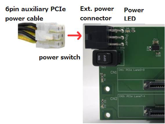

Figure-4: Power switch, PCIe auxiliary power supply, and its pin assignment
Access Indicator LED
@There is an SSD access LED near each U.2 connector as shown in Figure 5, which emits light when the respective U.2 connector pin P11 (ACTIVITY# signal) is at a Low level.
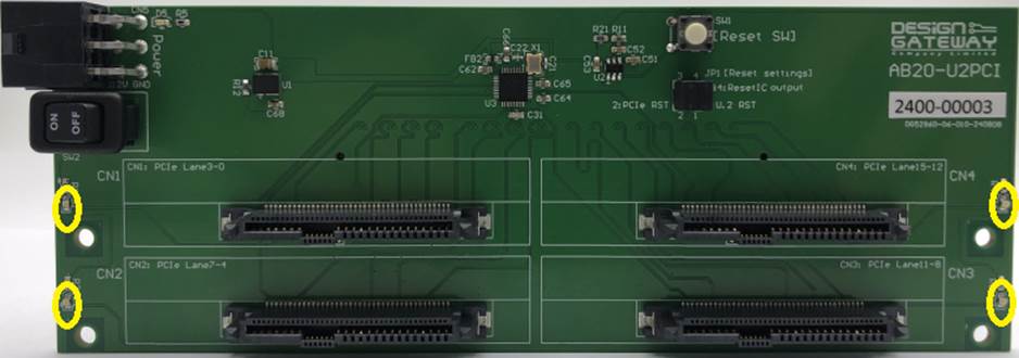
Figure-5: Access Indicator LED for each SSD (Yellow mark position)
Clock circuit
The adapter is equipped with a clock generator that complies with the PCI Express Gen5 standard and provides 100MHz differential clocks in the same phase for all PCIe clock (Pin# A13/A14) and all 4 channels of U.2 SSDs system clock (Pin# E7/E8). @The clock frequency is fixed at 100 MHz and cannot be changed.
Reset circuit
The adapter contains a reset IC that generates reset signals for PCIe and U.2, a reset switch for manually generating a reset signal, and 2x2 jumper headers for selecting each reset system.
The reset IC constantly monitors the voltage level of the +3.3V power supply and outputs a low active reset signal when the voltage level falls below approximately 3.0V. It also generates a reset signal pulse of about 100msec when the reset switch is pressed.
The reset signal connection can be set as shown below by inserting a socket into the 2 x 2 4-pin header JP1 shown in Figure 6. @(The factory default socket settings are the connections between 1-4 and between 2-3 as shown in Figure 6.)
Short between 1 and 4: Connects the reset IC output to the reset of all 4 U.2 SSDs (Pin# E5).
Short between 2 and 3: Connects the reset IC output to the PCI Express reset (Pin# A11)
Short between 1-2: Connects PCI Express reset (Pin#A11) to all 4 U.2 SSD resets (Pin#E5).
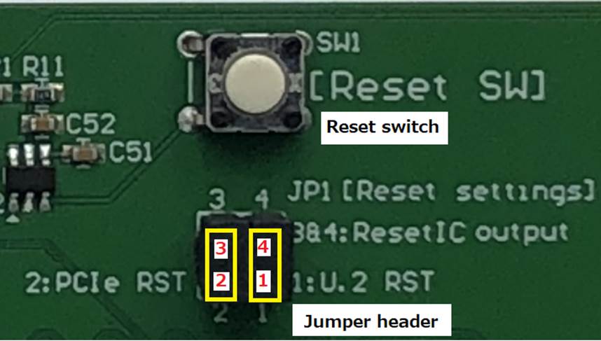
Figure-6: Reset switch (SW1) and pin header (JP1) for reset connection settings
Connection between PCIe and each U.2 SSD
The connection between each lane of the PCIe socket and the four U.2 SSDs attached to CN1-CN4 in this adapter is as follows
|
PCIe Lane# (signal direction) |
PCIe signal name |
PCIe Pin# |
U.2 Conn. |
U.2 Pin# |
|
Lane0 Tx (FPGA->PCIe->U.2) |
PERp0/PERn0 |
A16/A17 |
CN1 |
E10/E11 |
|
Lane0 Rx (FPGA<-PCIe<-U.2) |
PETp0/PETn0 |
B14/B15 |
CN1 |
E14/E13 |
|
Lane1 Tx (FPGA->PCIe->U.2) |
PERp1/PERn1 |
A21/A22 |
CN1 |
S17/S18 |
|
Lane1 Rx (FPGA<-PCIe<-U.2) |
PETp1/PETn1 |
B19/B20 |
CN1 |
S21/S20 |
|
Lane2 Tx (FPGA->PCIe->U.2) |
PERp2/PERn2 |
A25/A26 |
CN1 |
S23/S24 |
|
Lane2 Rx (FPGA<-PCIe<-U.2) |
PETp2/PETn2 |
B23/B24 |
CN1 |
S27/S26 |
|
Lane3 Tx (FPGA->PCIe->U.2) |
PERp3/PERn3 |
A29/A30 |
CN1 |
E17/E18 |
|
Lane3 Rx (FPGA<-PCIe<-U.2) |
PETp3/PETn3 |
B27/B28 |
CN1 |
E21/E20 |
|
Lane4 Tx (FPGA->PCIe->U.2) |
PERp4/PERn4 |
A35/A36 |
CN2 |
E10/E11 |
|
Lane4 Rx (FPGA<-PCIe<-U.2) |
PETp4/PETn4 |
B33/B34 |
CN2 |
E14/E13 |
|
Lane5 Tx (FPGA->PCIe->U.2) |
PERp5/PERn5 |
A39/A40 |
CN2 |
S17/S18 |
|
Lane5 Rx (FPGA<-PCIe<-U.2) |
PETp5/PETn5 |
B37/B38 |
CN2 |
S21/S20 |
|
Lane6 Tx (FPGA->PCIe->U.2) |
PERp6/PERn6 |
A43/A44 |
CN2 |
S23/S24 |
|
Lane6 Rx (FPGA<-PCIe<-U.2) |
PETp6/PETn6 |
B41/B42 |
CN2 |
S27/S26 |
|
Lane7 Tx (FPGA->PCIe->U.2) |
PERp7/PERn7 |
A47/A48 |
CN2 |
E17/E18 |
|
Lane7 Rx (FPGA<-PCIe<-U.2) |
PETp7/PETn7 |
B45/B46 |
CN2 |
E21/E20 |
|
Lane8 Tx (FPGA->PCIe->U.2) |
PERp8/PERn8 |
A52/A53 |
CN3 |
E10/E11 |
|
Lane8 Rx (FPGA<-PCIe<-U.2) |
PETp8/PETn8 |
B50/B51 |
CN3 |
E14/E13 |
|
Lane9 Tx (FPGA->PCIe->U.2) |
PERp9/PERn9 |
A56/A57 |
CN3 |
S17/S18 |
|
Lane9 Rx (FPGA<-PCIe<-U.2) |
PETp9/PETn9 |
B54/B55 |
CN3 |
S21/S20 |
|
Lane10 Tx (FPGA->PCIe->U.2) |
PERp10/PERn10 |
A60/A61 |
CN3 |
S23/S24 |
|
Lane10 Rx (FPGA<-PCIe<-U.2) |
PETp10/PETn10 |
B58/B59 |
CN3 |
S27/S26 |
|
Lane11 Tx (FPGA->PCIe->U.2) |
PERp11/PERn11 |
A64/A65 |
CN3 |
E17/E18 |
|
Lane11 Rx (FPGA<-PCIe<-U.2) |
PETp11/PETn11 |
B62/B63 |
CN3 |
E21/E20 |
|
Lane12 Tx (FPGA->PCIe->U.2) |
PERp12/PERn12 |
A68/A69 |
CN4 |
E10/E11 |
|
Lane12 Rx (FPGA<-PCIe<-U.2) |
PETp12/PETn12 |
B66/B67 |
CN4 |
E14/E13 |
|
Lane13 Tx (FPGA->PCIe->U.2) |
PERp13/PERn13 |
A72/A73 |
CN4 |
S17/S18 |
|
Lane13 Rx (FPGA<-PCIe<-U.2) |
PETp13/PETn13 |
B74/B75 |
CN4 |
S21/S20 |
|
Lane14 Tx (FPGA->PCIe->U.2) |
PERp14/PERn14 |
A76/A77 |
CN4 |
S23/S24 |
|
Lane14 Rx (FPGA<-PCIe<-U.2) |
PETp14/PETn14 |
B70/B71 |
CN4 |
S27/S26 |
|
Lane15 Tx (FPGA->PCIe->U.2) |
PERp15/PERn15 |
A80/A81 |
CN4 |
E17/E18 |
|
Lane15 Rx (FPGA<-PCIe<-U.2) |
PETp15/PETn15 |
B78/B79 |
CN4 |
E21/E20 |
Table-1:
Connection between each PCIe lane and four U.2 SSDs
Disclaimer
Any damage to the FPGA evaluation board or SSD device caused by misuse of this adapter will be exempted from any and all liability. @In addition, this adapter board is for evaluation purposes only, and may not operate properly depending on the characteristics of the FPGA evaluation board or the SSD device to which it is connected, but this is an exemption from liability except for manufacturing defects in the adapter board.
[Contact]
URL : https://dgway.com/index_E.html
Email : info@dgway.com
Revision History
|
Revision |
Date |
Description |
|
1.0E |
Oct-7th-2024 |
English manual first release |
|
|
|
|