This document describes the FPGA and environment setup for running NVMe-IP RAID0 demo on FPGA development board by using the PCIe adapter board (AB18-PCIeX16 adapter board) with four M.2 NVMe SSDs for RAID0 operation. User controls the test operation via NiosII command shell.
1 Environment Requirement
To run the demo on FPGA development board, please prepare following environment.
1) Supported FPGA Development board:
NVMe-IP for Agilex: Agilex F-series Development board (PCIe Gen4)
2) PC installing QuartusII programmer and NiosII command shell software
3) The PCIe adapter board (AB18-PCIeX16), provided by Design Gateway
https://dgway.com/ABseries_E.html
4) Intel power adapter for FPGA board
5) ATX power supply for AB18-PCIeX16 adapter board
6) Ultra Quad M.2 Card, connecting B side (Device) of AB18. https://www.asrock.com/mb/spec/product.asp?Model=ULTRA%20QUAD%20M.2%20CARD
7) Four M.2 NVMe SSDs
8) Micro USB cable for FPGA programming/NiosII command shell, connecting between FPGA board and PC.
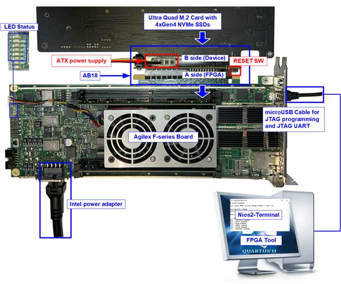
Figure 1‑1 NVMe-IP demo setup on Agilex F-series Development board (PCIe Gen4)
2 Demo setup
2.1 Board setup
1) Power off system.
2) Connect four M.2 NVMe SSDs to four connectors on Ultra Quad M.2 Card, as shown in Figure 2‑1.
Agilex F-series development board: NVMe Gen4 SSD
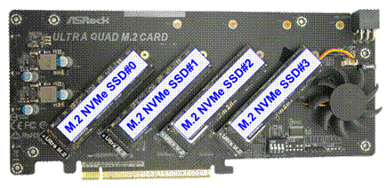
Figure 2‑1 Four M.2 NVMe Gen4 SSDs with Ultra Quad M.2 Card
3) Connect AB18 to FPGA board by following step.
i) Connect ATX power to ATX power connector on AB18-PCIeX16 board.
ii) Connect FPGA side (A-side) of PCIe connector on AB18-PCIeX16 board to PCIe connector on FPGA board
iii) Check that two mini jumpers are inserted at J5 connector on AB18
iv) Connect Quad M.2 NVMe SSD Card to Device side (B-side) of PCIe connector on AB18-PCIeX16 board
Warning: Please confirm that the Quad M.2 Card is inserted in the correct side of AB18 (B-side, not A-side) before power on system.
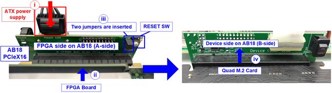
Figure 2‑2 Connect PCIe connector between AB18 and FPGA board
4) Connect micro USB for JTAG programming and NiosII command shell.
5) Connect FPGA power adapter to FPGA board.
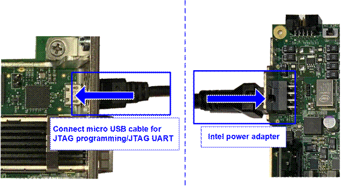
Figure 2‑3 Connect USB cable and power adapter to FPGA board
6) Turn on power switch of FPGA development board, AB18-PCIeX16 board, and ATX power supply.
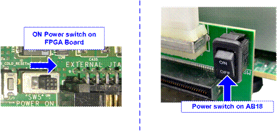
Figure 2‑4 Power on FPGA board and AB18 board
2.2 Program setup
1) Use QuartusII Programmer to program �NVMeRaid0x4Test_xxx.sof� file, as shown in Figure 2‑5.
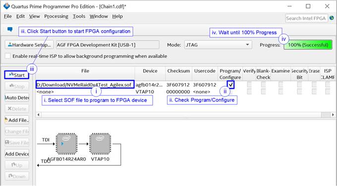
Figure 2‑5 Programmed by QuartusII Programmer
2) Open NiosII Command Shell and run �nios2-terminal� command. After that, boot message is displayed.
i. �Waiting PCIe Linkup� is displayed when CPU monitors linkup signal of PCIe-IP.
ii. �Waiting IP initialization� is displayed after PCIe-IP linkup. Next, CPU waits until NVMe-IP initialization finished.
iii. �Ch[#]PCIe Gen4 (or 3/2/1) x4 (or x2/x1) Device Detect� shows PCIe speed and number of PCIe lane after finishing IP initialization process.
iv. Finally, Main menu is displayed to receive command from user.
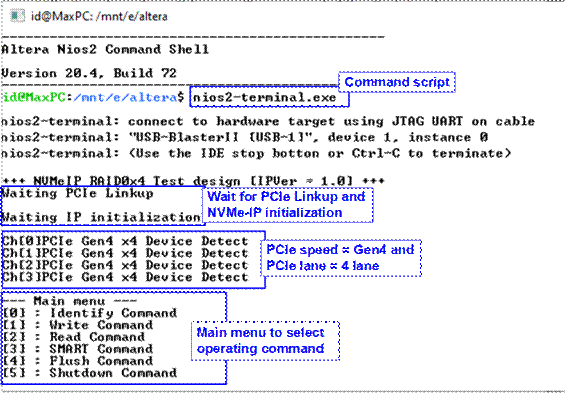
Figure 2‑6 NiosII Terminal
3) Check LED status on FPGA board. The description of LED is shown as follows.
Table 2‑1 LED Definition
|
GPIO LED |
ON |
OFF |
|
0 |
Normal operation |
Clock is not locked |
|
1 |
System is busy |
Idle status |
|
2 |
PCIe Error detect |
Normal operation |
|
3 |
Data verification fail |
Normal operation |
4) After programming completely, LED[0] and LED[1] are ON. LED[1] is OFF after RAID0 completes initialization process. Finally, the system is ready to receive command from user.
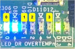
Figure 2‑7 LED Status for user output
3 Revision History
|
Revision |
Date |
Description |
|
1.0 |
24-Jun-21 |
Initial version release |