FPGA Setup for NVMe-IP/NVMeG3-IP demo
Rev4.2 3-Jul-23
2.1.1 TR-5 Lite Development board by AB18 and ATX power supply
2.1.3 Arria10 SoC Development board
This document describes the FPGA and environment setup for running NVMe-IP or NVMeG3-IP demo on FPGA development board by using the PCIe adapter board (AB18-PCIeX16 or AB16-PCIeXOVR adapter board) with NVMe SSD. User controls the test operation via NiosII command shell.
1 Environment Requirement
To run the demo on FPGA development board, please prepare following environment.
1) Supported FPGA Development board:
NVMe-IP:
- ArriaV GX Starter board (PCIe Gen2)
- Cyclone10 GX Development board (PCIe Gen2)
- TR5-Lite Development board (PCIe Gen3)
- Arria10 SoC Development board (PCIe Gen3)
- Arria10 GX Development board (PCIe Gen3)
- Alaric board (PCIe Gen3)
- Stratix10 GX Development board (PCIe Gen3)
- Agilex F-series Development board (PCIe Gen4)
NVMeG3-IP:
- Arria10 GX Development board (PCIe Gen3)
2) PC installing QuartusII programmer and NiosII command shell software
3) The PCIe adapter board (AB18-PCIeX16 or AB16-PCIeXOVR), provided by Design Gateway
https://dgway.com/ABseries_E.html
4) Intel power adapter for FPGA board
5) ATX power supply for AB18-PCIeX16 adapter board
6) NVMe SSD connecting with PCIe adapter board
7) A cable for FPGA programming/NiosII command shell, connecting between FPGA board and PC.
a) ArriaV GX Starter board: USB A-B cable
b) TR5-Lite board: USB A-B cable and USB Blaster
c) Cyclone10GX, Arria10 SoC, Arria10 GX, Alaric board, Stratix10 GX board, and Agilex F-series: micro USB cable
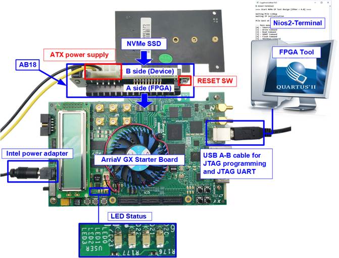
Figure 1‑1 NVMe-IP demo setup on ArriaV GX Starter board (PCIe Gen2)
Figure 1‑2 NVMe-IP demo setup on TR-5 Lite Development board (PCIe Gen3)
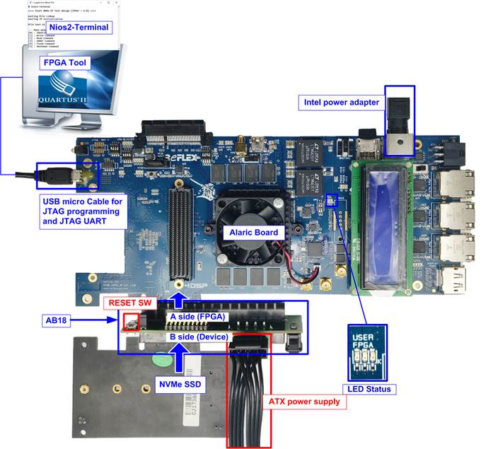
Figure 1‑3 NVMe-IP demo setup on Alaric board (PCIe Gen3)
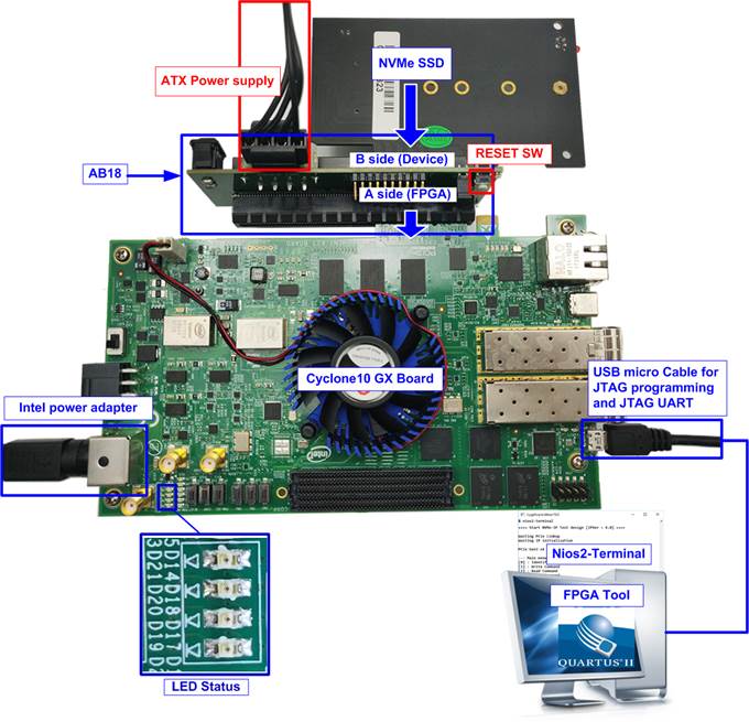
Figure 1‑4 NVMe-IP demo setup on Cyclone10 GX board (PCIe Gen2)
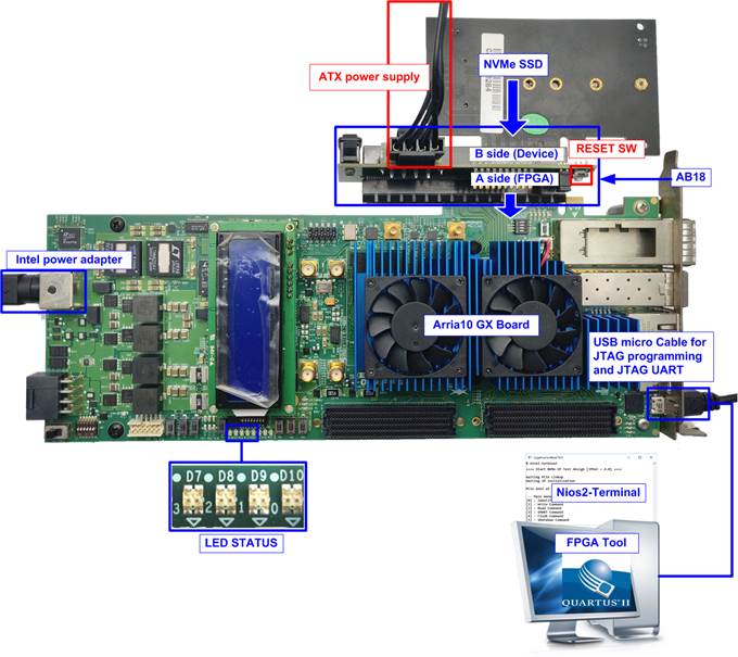
Figure 1‑5 NVMe-IP/NVMeG3-IP demo setup on Arria10 GX Development board (PCIe Gen3)
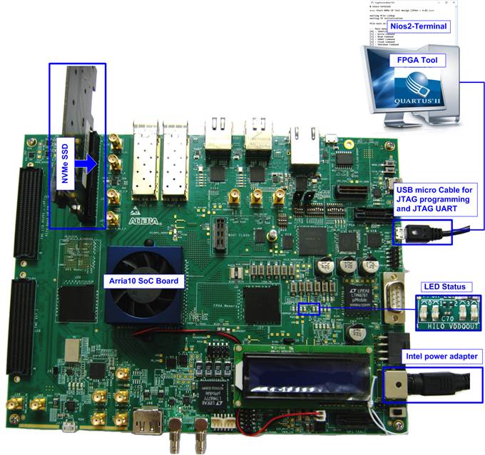
Figure 1‑6 NVMe-IP demo setup on Arria10 SoC Development board (PCIe Gen3)
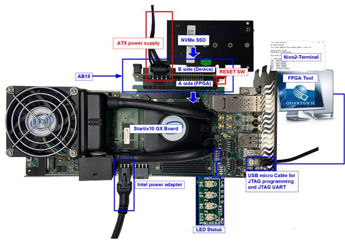
Figure 1‑7 NVMe-IP demo setup on Stratix10 GX Development board (PCIe Gen3)
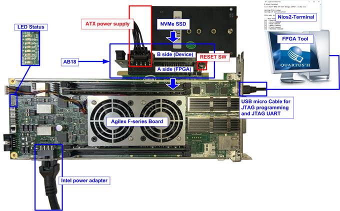
Figure 1‑7 NVMe-IP demo setup on Agilex F-series Development board (PCIe Gen4)
2 Demo setup
2.1 Board setup
2.1.1 TR-5 Lite Development board by AB18 and ATX power supply
1) Power off system.
2) Connect ATX power supply to FPGA board.
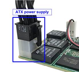
Figure 2‑1 ATX power supply connected to FPGA
3) Connect AB18/AB16, SSD, and FPGA board by following steps.
i. Connect A Side of PCIe connector on AB18/AB16 board to PCIe connector on FPGA board.
ii. Check that two mini jumpers are inserted at J5 connector on AB18/AB16 board.
iii. Connect NVMe SSD to B Side of PCIe connector on AB18/AB16 board.
iv. Connect ATX power supply to AB18/AB16 board as shown in Figure 2‑2.
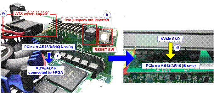
Figure 2‑2 Connect PCIe connector between AB18/AB16 and FPGA board
4) Connect USB cable to FPGA board by following steps.
i. Connect USB Blaster cable to FPGA board for JTAG programming/NiosII command shell.
ii. Connect USB A-B cable to USB Blaster, as shown in Figure 2‑3.
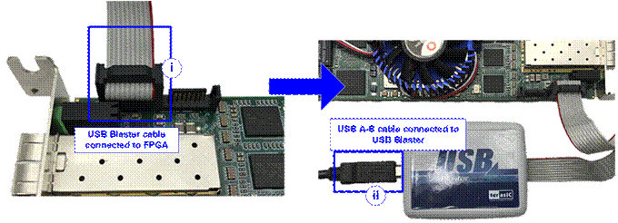
Figure 2‑3 USB cable connection
5) Turn on power switch of ATX power supply and AB18/AB16 board.
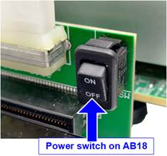
Figure 2‑4 Power on AB18/AB16 board
2.1.2 Arria10 GX/Cyclone10GX/Alaric board/ArriaV GX/Stratix10 GX/Agilex F-series by AB18 and ATX power supply
1) Power off system.
2) Connect AB18/AB16, SSD, and FPGA board by following steps.
i. Connect ATX power to ATX power connector on AB18-PCIeX16 board.
ii. Connect A Side of PCIe connector on AB18-PCIeX16 board to PCIe connector on FPGA board
iii. Check that two mini jumpers are inserted at J5 connector on AB18
iv. Connect NVMe SSD to B Side of PCIe connector on AB18-PCIeX16 board
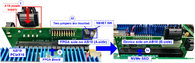
Figure 2‑5 Connect PCIe connector between AB18 and FPGA board
3) For JTAG programming and NiosII command shell,
a. Arria10 GX, Cyclone10GX, Alaric board, Stratix10GX, and Agilex F-series: Connect micro USB cable from FPGA board to PC
b. ArriaV GX: Connect USB A-B cable from FPGA board to PC
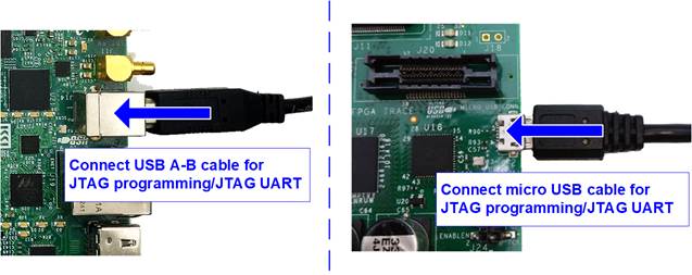
Figure 2‑6 Connect USB cable to FPGA board
4) Connect FPGA power adapter to FPGA board.
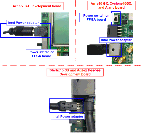
Figure 2‑7 Connect Intel power adapter to FPGA board
5) Turn on power switch of FPGA development board, AB18-PCIeX16 board and ATX power supply.
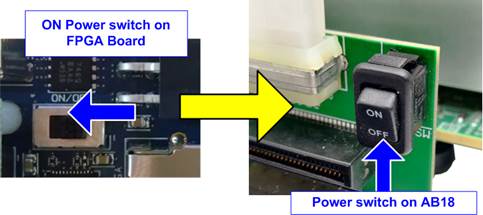
Figure 2‑8 Power on FPGA board and AB18 board
2.1.3 Arria10 SoC Development board
1) Power off system.
2) Connect NVMe SSD to PCIe connector on FPGA board, as shown in Figure 2‑9.
3) Connect micro USB cable from FPGA board to PC for JTAG programming/NiosII command shell.
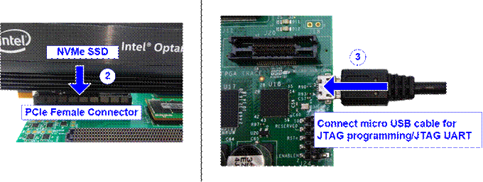
Figure 2‑9 NVMe PCIe SSD connection on FPGA board
4) Set SW1[2] = OFF position to source power to the PCIe, as shown in Figure 2‑10.
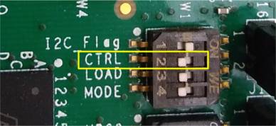
Figure 2‑10 Source power to the PCIe for Arria10 SoC board
5) Connect FPGA power adapter to FPGA board and power on FPGA development board.
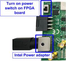
Figure 2‑11 Connect Intel power adapter on Arria10 SoC board
2.2 Program setup
1) Use QuartusII Programmer to program �NVMeIPTest_xxx.sof� file, as shown in Figure 2‑12.
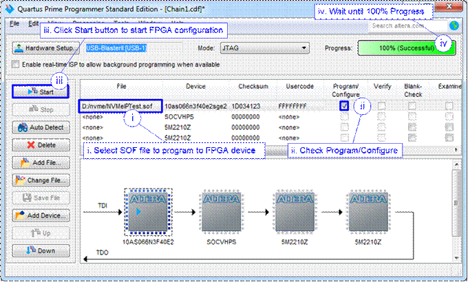
Figure 2‑12 Programmed by QuartusII Programmer
2) Open NiosII Command Shell and run �nios2-terminal� command. After that, boot message is displayed.
i. �Waiting PCIe Linkup� is displayed when CPU monitors linkup signal of PCIe-IP.
ii. �Waiting IP initialization� is displayed after PCIe-IP linkup. Next, CPU waits until NVMe-IP initialization finished.
iii. �PCIe Gen3 (or 4/2/1) x4 (or x2/x1) Device Detect� shows PCIe speed and PCIe lane after finishing IP initialization process.
iv. Finally, Main menu is displayed to receive command from user.
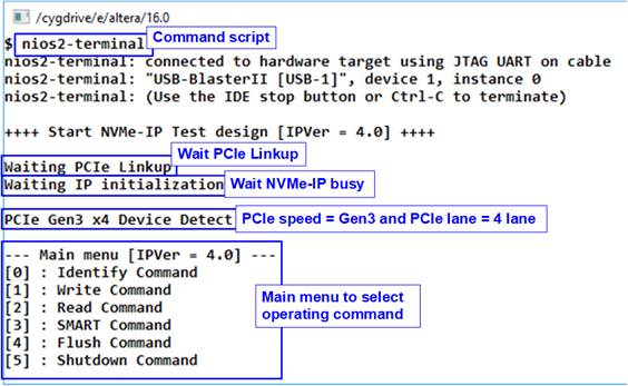
Figure 2‑13 NiosII Terminal
3) Check LED status on FPGA board. The description of LED is shown as follows.
Note: There are three LEDs on Alaric board. Therefore, LED3 is not available.
Table 2‑1 LED Definition
|
GPIO LED |
ON |
OFF |
|
0 |
Normal operation |
Clock is not locked |
|
1 |
System is busy |
Idle status |
|
2 |
PCIe Error detect |
Normal operation |
|
3 |
Data verification fail |
Normal operation |
4) After programming completely, LED[0] and LED[1] are ON when PCIe initialization is processing. LED[1] is OFF after PCIe completes initialization process. Finally, the system is ready to receive command from user.
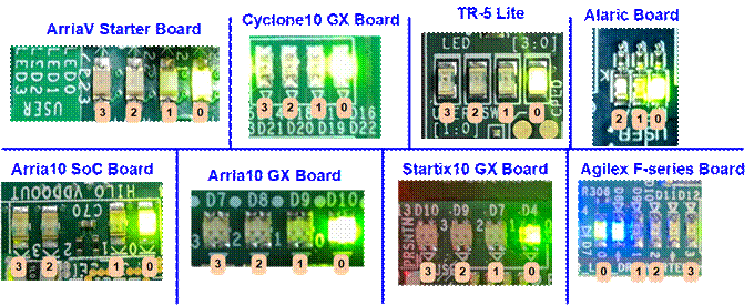
Figure 2‑14 LED Status for user output
3 Revision History
|
Revision |
Date |
Description |
|
1.0 |
9-Aug-16 |
Initial version release |
|
1.1 |
17-Aug-16 |
Update message during write/read command |
|
1.2 |
19-Dec-16 |
Update performance result of new buffer system |
|
1.3 |
20-Mar-17 |
Support Arria10 GX Development board |
|
1.4 |
9-May-17 |
Update SSD model and test result for new IP version |
|
2.0 |
8-Jun-17 |
Support only 256 Kbyte buffer |
|
2.1 |
31-Jul-17 |
Add LFSR pattern |
|
2.2 |
25-Sep-17 |
Support Alaric board |
|
2.3 |
27-Oct-17 |
Change PCIe connector on Alaric board |
|
3.0 |
20-Jul-18 |
Support Shutdown, SMART, and Flush command |
|
3.1 |
12-Feb-20 |
Support Cyclone10GX and AB18-PCIeX16 board |
|
3.2 |
20-Apr-20 |
Remove PCIeSub board support of AB18 |
|
4.0 |
13-Jul-20 |
Remove instruction from the document and include NVMeG3-IP |
|
4.1 |
24-Sep-20 |
Support Stratix10GX board |
|
4.2 |
1-Jun-21 |
Support Agilex F-series board (PCIe Gen4) |