NVMeSW IP Core Demo Instruction
Rev1.2 17-Aug-23
This document describes the instruction to run NVMeSW-IP demo on FPGA development board by using the PCIe adapter board (AB18-PCIeX16 board or AB16-PCIeXOVR board). The demo is designed to write/verify data by connecting NVMe SSD through PCIe switch. User controls the test operation through Serial console.
The sequence to run NVMeSW-IP with NVMe SSD directly without PCIe switch is mostly similar to NVMe-IP. So, please see more details of direct connection from “NVMe-IP demo Instruction” document.
https://dgway.com/products/IP/NVMe-IP/dg_nvmeip_instruction_v4_en.pdf
1 Environment Requirement
To run the demo on FPGA development board, please prepare following environment.
1) Supported FPGA Development board: KCU105/ZCU106/VCU118
2) PC installing Xilinx programmer software (Vivado) and Serial console software such as HyperTerminal and TeraTerm
3) The PCIe adapter board (AB18-PCIeX16 board/AB16-PCIeXOVR board) provided by Design Gateway
https://dgway.com/ABseries_E.html
4) Xilinx power adapter for FPGA board
5) ATX power supply for PCIe adapter board
6) PCIe switch card with M.2 connector such as
a) Quattro 400 M.2 NVMe SSD adapter
https://www.aplicata.com/quattro-400/
b) Squid SKU-086-34 NVMe SSD Adapter
https://amfeltec.com/products/pci-express-gen-3-carrier-board-for-m-2-ssd/
7) 1-4 NVMe SSDs connecting on PCIe switch card
8) Two micro USB cables connecting between FPGA board and PC (one for programming FPGA and another for Serial console)
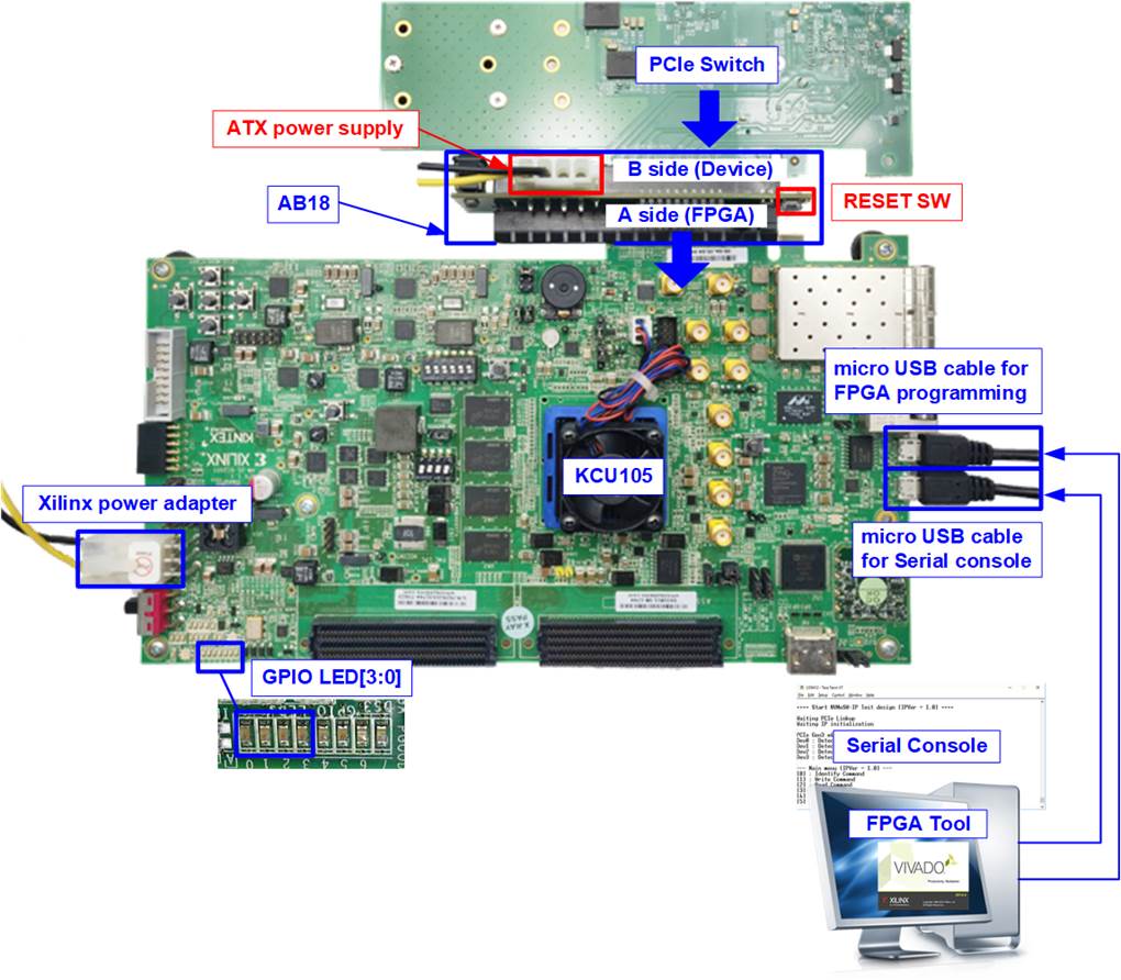
Figure 1‑1 NVMeSW-IP demo environment setup on KCU105
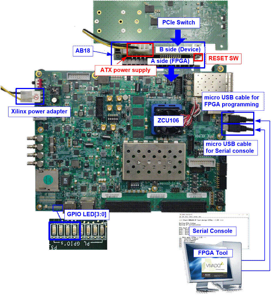
Figure 1‑2 NVMeSW-IP demo environment setup on ZCU106
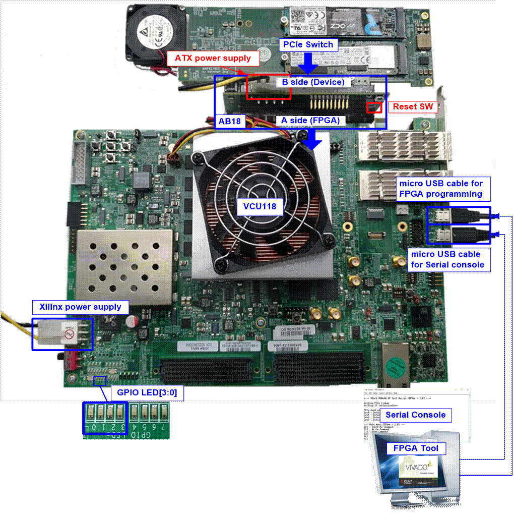
Figure 1‑3 NVMeSW-IP demo environment setup on VCU118
2 Demo setup
1) Power off system.
2) For ZCU106 board, set SW6[4:1] = all ON to configure PS from JTAG, as shown in Figure 2‑1.
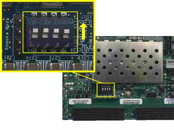
Figure 2‑1 SW6 setting to configure PS from JTAG on ZCU106
3) Connect ATX power supply to AB18-PCIeX16 board and Xilinx power adapter to FPGA development board.
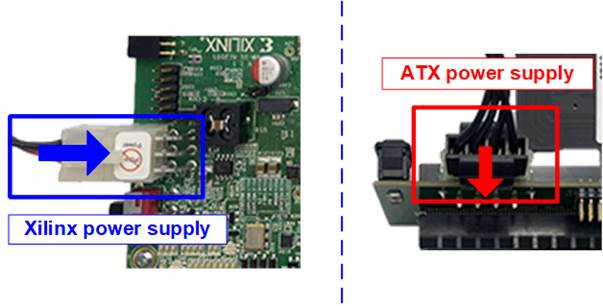
Figure 2‑2 Power connection
4) Connect 1-4 NVMe SSDs to PCIe switch card. Figure 2‑3 and Figure 2‑4 show the example of using four SSDs connected to PCIe switch card.
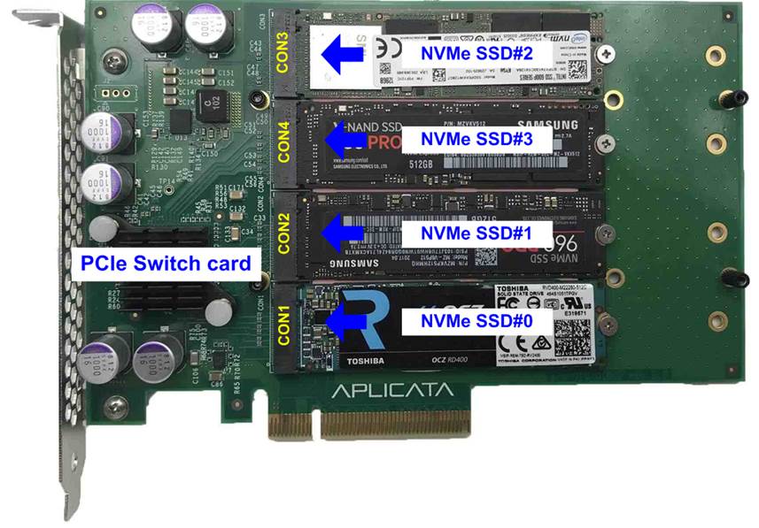
Figure 2‑3 Connect NVMe SSD to PCIe Swtich#1
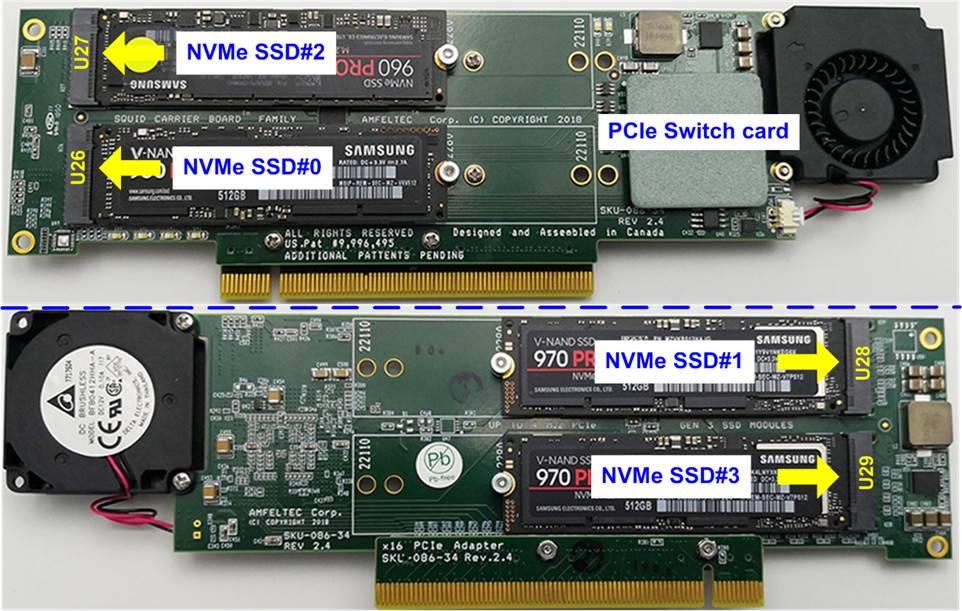
Figure 2‑4 Connect NVMe SSD to PCIe Swtich#2
5) a. Confirm that two mini jumpers are inserted at J5 connector on AB18.
b. Connect FPGA Side (A-side) on AB18 to PCIe connector on FPGA board
c. Connect PCIe switch to device side (B-Side) on AB18, as shown in Figure 2‑5.
Warning: Please confirm that the PCIe switch is inserted in the correct side of AB18 (B-side, not A-side) before power on system.
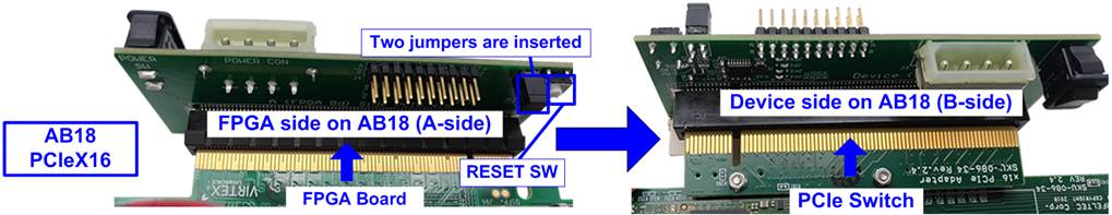
Figure 2‑5 Connect AB18 to PCIe switch and FPGA board
6) Connect two micro USB cables for JTAG programming and Serial console.
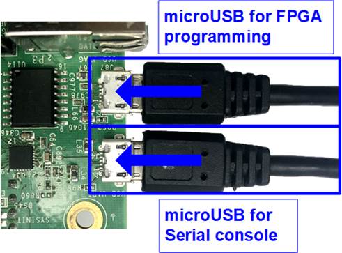
Figure 2‑6 USB cable connection
7) Power on FPGA development board, ATX power supply, and AB18 board, as shown in Figure 2‑7.
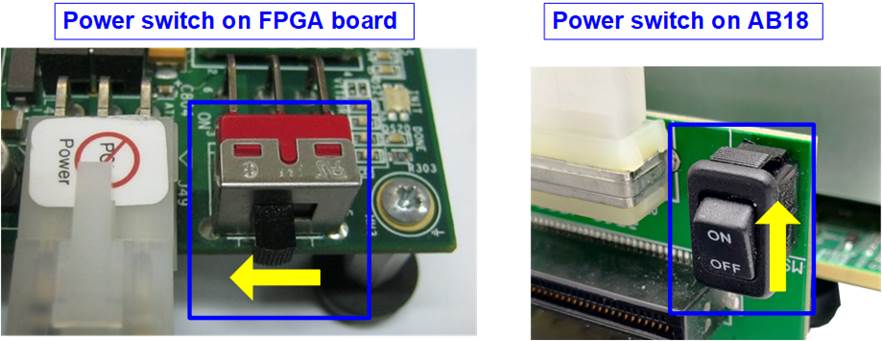
Figure 2‑7 Turn on power switch on FPGA and AB18 board
8) On PC, additional COM port is detected after connecting USB cables to FPGA board. On Ultrascale/Ultrascale+ board, more than one COM ports are detected.
In case of KCU105 and VCU118, select Standard COM port.
In case of ZCU106, select the lowest number for ZCU106 board, as shown in Figure 2‑8.
On Serial console, the setting is as follows. Buad rate=115,200, Data=8-bit, Non-Parity, and Stop = 1.
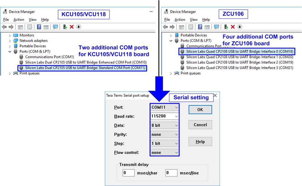
Figure 2‑8 Select and set COM port
9) Download and program configuration file and firmware to FPGA board.
a) For KCU105/VCU118, configure FPGA by using Vivado as shown in Figure 2‑9.
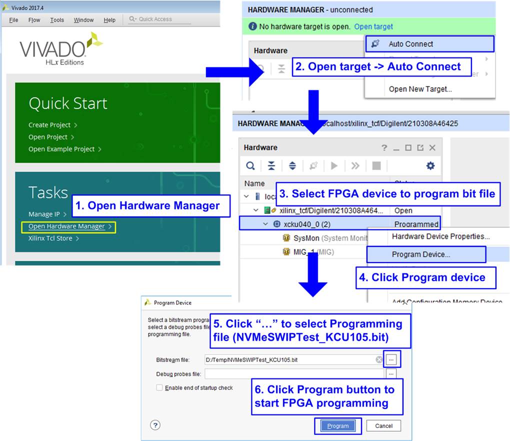
Figure 2‑9 Program FPGA by Vivado
b) For ZCU106 board, open Vivado TCL shell, change directory to ready_for_download or directory that batch file is located. Next, type NVMeSWIPTest_ZCU106.bat, as shown in Figure 2‑10.
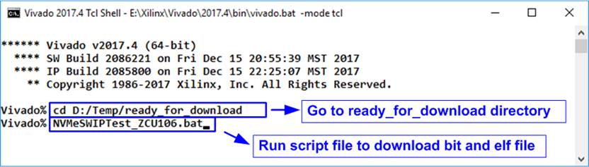
Figure 2‑10 Command script to download demo file on Vivado TCL shell
10) Check LED status on FPGA board. The description of LED is as follows.
Table 2‑1 LED Definition
|
GPIO LED |
ON |
OFF |
|
0 |
Normal operation |
Clock is not locked or reset button is pressed |
|
1 |
System is busy |
Idle status |
|
2 |
IP Error detect |
Normal operation |
|
3 |
Data verification fail |
Normal operation |
11) After finishing FPGA programming, LED[0] and LED[1] are ON during PCIe initialization process. LED[1] changes to OFF after PCIe initialization process is finished as shown in Figure 2‑11.
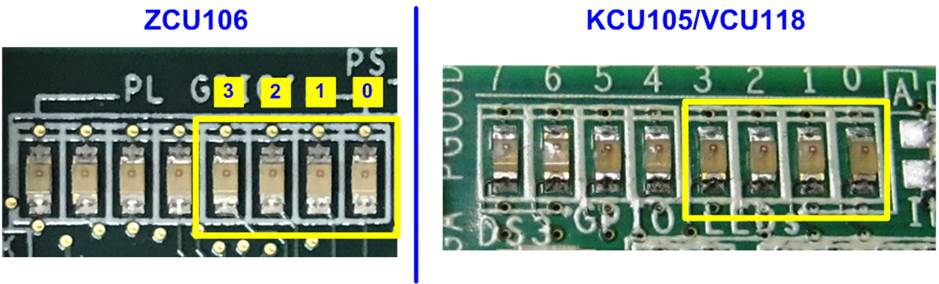
Figure 2‑11 Four LEDs to show the current status
12) On the console, the message is displayed to show current status as follows.
· “Waiting PCIe Linkup” is displayed after finishing configuration.
· After PCIe is linkup, “Waiting IP initialization” is displayed.
· After finishing NVMeSW-IP initialization, PCIe speed, number of PCIe lanes, and total detected devices are displayed. Finally, main menu to run six commands is shown on the console. The example message when connecting to four SSDs and one SSD is shown in Figure 2‑12.
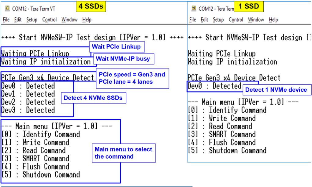
Figure 2‑12 Main menu after IP finishes initialization
3 Test Menu
3.1 Identify Command
Select ‘0’ to send Identify command to NVMe SSD.
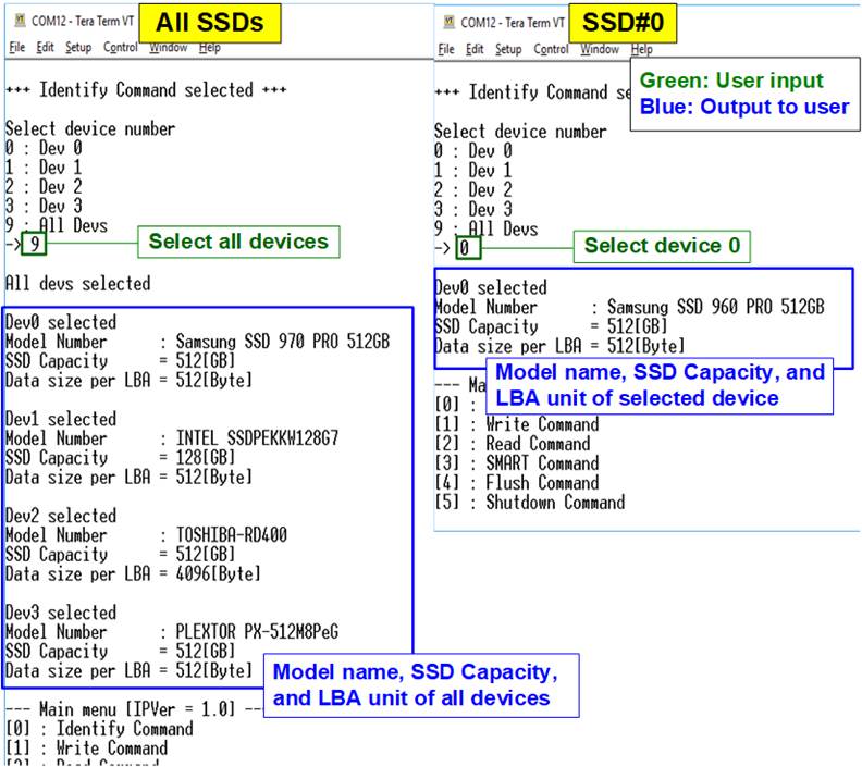
Figure 3‑1 Test result when running Identify command
After that, user inputs to select the active device.
Input ‘9’ to run the command to all devices in the system or 0-3 to run only one device.
If the input is valid, the SSD information output from Identify command is displayed as shown in Figure 3‑1. The console shows three values for each SSD.
1) SSD model number: This value is decoded from Identify controller data.
2) SSD capacity: This value is signal output from IP.
3) Data size per LBA: This value is signal output from IP. Two values are supported, i.e. 512 byte and 4 Kbyte.
If user selects the unavailable device, error message is displayed as shown in Figure 3‑2.
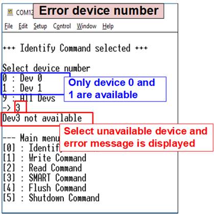
Figure 3‑2 Error message when selecting the unavailable device
3.2 Write Command
Select ‘1’ to send Write command to NVMe SSD.
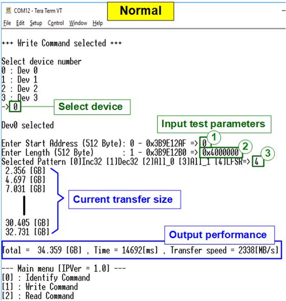
Figure 3‑3 Test result when running Write command
The first input from user is the device selection. User must input the device number for running Write command. If the input is valid, the selected device number is displayed on the console.
Next, user inputs three parameters as follows.
1) Start Address: Input start address to write SSD as 512-byte unit. The input is decimal unit when user enters only digit number. User can add “0x” to be a prefix for hexadecimal unit. When LBA unit of SSD is 4 Kbyte, this input must be aligned to 8.
2) Transfer Length: Input total transfer size as 512-byte unit. The input is decimal unit when user enters only digit number. User can add “0x” to be a prefix for hexadecimal unit. When LBA unit of SSD is 4 Kbyte, this input must be aligned to 8.
3) Test pattern: Select test data pattern for writing to SSD. There are five patterns, i.e. 32-bit incremental, 32-bit decremental, all-0, all-1, and 32-bit LFSR counter.
When all inputs are valid, the operation begins. During writing data, current transfer size is displayed on the console every second to show that system is still alive. Finally, total size, total time usage, and test speed are displayed on the console to be a test result.
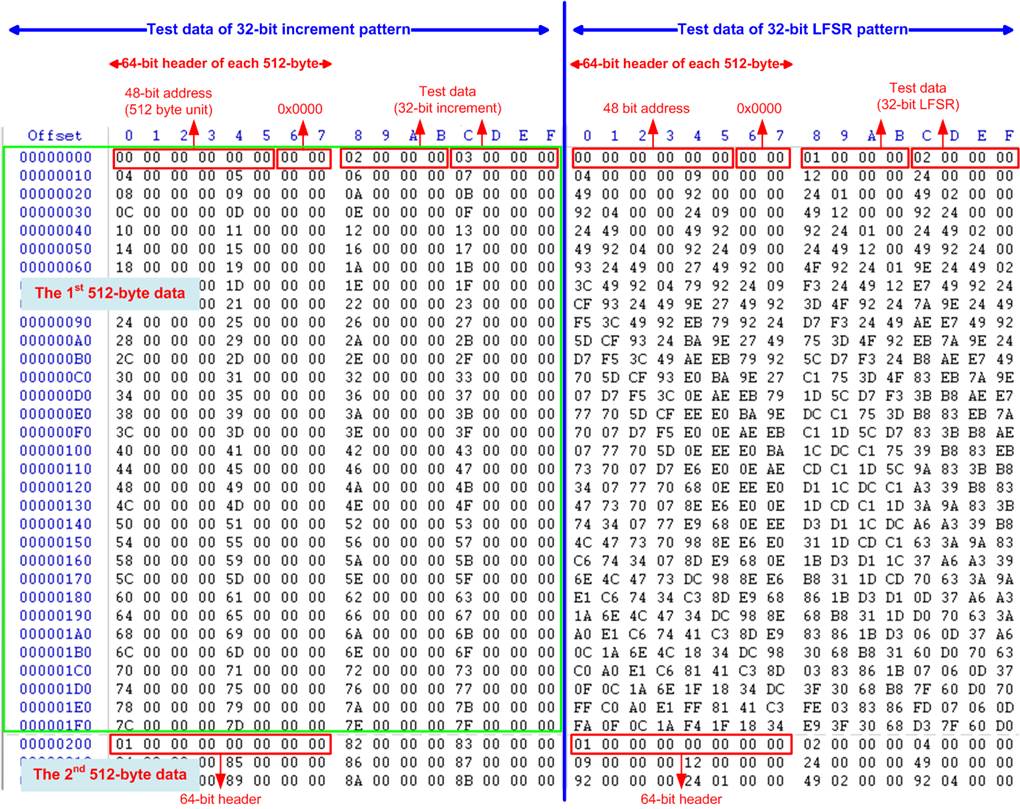
Figure 3‑4 Example Test data of the 1st and 2nd 512-byte by using increment/LFSR pattern
Test data in SSD is split into 512-byte unit. For incremental, decremental, or LFSR pattern, each 512-byte data has unique 64-bit header consisting of 48-bit address (in 512-byte unit) and 16-bit zero value. The data after 64-bit header is the test pattern which is selected by user.
The left window of Figure 3‑4 shows the example when using 32-bit incremental pattern while the right window shows the example when using 32-bit LFSR pattern. The unique header is not included when running all-0 or all-1 pattern.
When user runs Write or Read command with 4-Kbyte LBA SSD, there is the message displaying on the console to show the input limitation which must be aligned to 8, as shown in Figure 3‑5. When the input does not align to 8, “Invalid input” is displayed and the operation is cancelled.
Also, Figure 3‑6 shows the example when the input is out of the recommended range for each parameter. The console displays “Invalid input” and then the operation is cancelled.
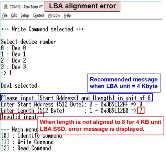
Figure 3‑5 Error message when the input is unaligned for SSD with 4KB LBA unit

Figure 3‑6 Error message from the invalid input
3.3 Read Command
Select ‘2’ to send Read command to NVMe SSD.
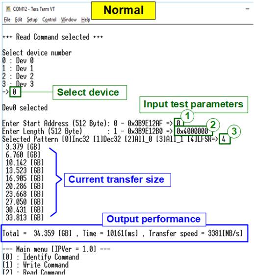
Figure 3‑7 Test result when running Read command
The first input from user is the device selection. User must input the device number for running Read command. If the input is valid, the selected device number is displayed on the console.
Next, user inputs three parameters as follows.
1) Start Address: Input start address to read SSD as 512-byte unit. The input is decimal unit when user enters only digit number. User can add “0x” to be a prefix for hexadecimal unit. When LBA unit of SSD is 4 Kbyte, this input must be aligned to 8.
2) Transfer Length: Input total transfer size as 512-byte unit. The input is decimal unit when user enters only digit number. User can add “0x” to be a prefix for hexadecimal unit. If LBA unit of SSD is 4 Kbyte, this input must be aligned to 8.
3) Test pattern: Select test data pattern to verify data from SSD. Test pattern must be matched with the pattern using in Write Command menu. There are five patterns, i.e. 32-bit incremental, 32-bit decremental, all-0, all-1, and 32-bit LFSR counter.
Similar to Write command menu, test system reads data from SSD when all inputs are valid. During reading data, current transfer size is displayed on the console every second to show that system is still alive. Total size, total time usage, and test speed are displayed after finishing the operation.
“Invalid input” is displayed when some inputs are invalid or unaligned to 8 (when connecting to 4-KB LBA SSD).
“Invalid input” is displayed when some inputs are invalid or unaligned to 8 (when connecting to 4-KB LBA SSD).
Figure 3‑8 shows error message when data verification is failed. “Verify fail” is displayed with the information of the 1st failure data, i.e. the error byte address, the expected value, and the read value.
User can press any key(s) to cancel read operation or wait until finishing Read command. Similar to the normal condition, the output performance is displayed on the console when the user does not enter any key(s) to stop the operation.
When cancelling the operation, the read command still runs as the background process. It is recommended to power-off/on AB18/AB16, and then press “RESET” button to restart system.

Figure 3‑8 Data verification is failed
3.4 SMART Command
Select ‘3’ to send SMART command to NVMe SSD.

Figure 3‑9 Test result when running SMART command
After that, user inputs to select the active device.
Input ‘9’ to run the command to all devices in the system or 0-3 to run only one device.
If the input is valid, the SSD SMART/health information (output from SMART command) us displayed as shown in Figure 3‑9. The console shows six parameters, described as follows.
1) Temperature in °C unit.
2) Total Data Read decoded as GB/TB unit. Additionally, raw data without decoding is displayed in 128-bit hexadecimal unit. The unit size of raw data is 512,000 byte.
3) Total Data Written decoded as GB/TB unit. Additionally, raw data without decoding is displayed in 128-bit hexadecimal unit. The unit size of raw data is 512,000 byte.
4) Power On Cycles: Display the number of power cycles.
5) Power On Hours: Display period of time in hours to show how long the SSD has been powered on.
6) Unsafe Shutdowns: Display the number of unsafe shutdowns of SSD
3.5 Flush Command
Select ‘4’ to send Flush command to NVMe SSD.
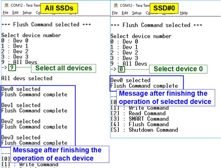
Figure 3‑10 Test result when running Flush command
After that, user inputs to select the active device.
Input ‘9’ to run the command to all devices in the system or 0-3 to run only one device.
When the input is valid, Flush command operation begins.
“Flush Command Complete” is displayed after finishing Flush operation.
3.6 Shutdown Command
Select ‘5’ to send Shutdown command to NVMe SSD.
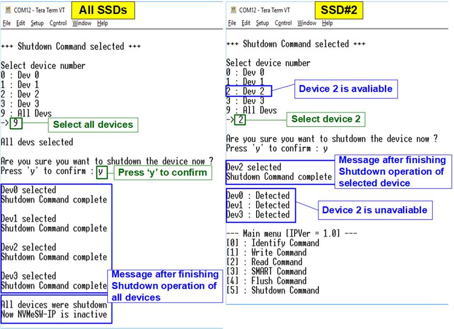
Figure 3‑11 Test result when running Shutdown Command
After that, user inputs to select the active device.
Input ‘9’ to run the command to all devices in the system or 0-3 to run only one device.
Next, the confirmation message is displayed on the console. User inputs ‘y’ or ‘Y’ to start Shutdown operation or inputs other keys to cancel the operation.
After finishing Shutdown operation, “Shutdown Command Complete” is displayed on the console. As shown in the left side of Figure 3‑11, if all devices are selected, the last message is “Now NVMeSW-IP is inactive”. No main menu is displayed after finishing the operation. The user needs to shut down the system.
As shown in the right side of Figure 3‑11, if one device is selected, the updated device list is displayed. The device which has just finished Shutdown command is not available in the list. User needs to re-power the system to wake up the SSD.
4 Revision History
|
Revision |
Date |
Description |
|
1.0 |
26-Apr-19 |
Initial version release |
|
1.1 |
14-Feb-20 |
Support AB18 |
|
1.2 |
20-Apr-20 |
Remove power adapter cable from AB18 |