FPGA Setup of FTP Server by muNVMe-IPG4 Demo
1 Overview
This document provides a comprehensive guide for setting up an FPGA board to demonstrate the FTP server by muNVMe-IP (Gen4) demo. It includes step-by-step instructions for connecting an NVMe SSD to the FPGA board and linking the FPGA board to the network via 100G Ethernet to function as an FTP server. Users will configure FTP server parameters and monitor operations via a Serial console.
Before running the FTP server demo, ensure the following hardware components are prepared and configured.
1) FPGA development board: VCK190
2) PC with FPGA programming tools (e.g., Vivado) and Serial console application (e.g., HyperTerminal or TeraTerm)
3) PC with a 100 Gigabit Ethernet card that supports RS-FEC.
4) 100G Ethernet cable: 2xQSFP28 transceiver (100GBASE-SR) and MPO to MPO cable
5) PCIe adapter board from Design Gateway for SSD connection
https://dgway.com/ABseries_E.html
· AB18-PCIeX16: For Add-In Card (AIC) form factor SSD.
· AB19-M2PCI: For M.2 SSD at CN#1
· AB20-U2PCI: For U.2 SSD at CN#1
6) Power adapter for the FPGA board
7) ATX power supply for the PCIe adapter board
8) NVMe Gen4 SSD connected to the PCIe adapter board
9) USB type-C cable for JTAG programming and Serial console communication.
Note: Additional Hardware References
· 100G Network Adapter: Nvidia MCX614106A-CCAT
https://docs.nvidia.com/networking/display/ConnectX6EN
· Ethernet Cable:
QSFP28 Transceiver: AMQ28-SR4-M1
https://www.sfpcables.com/100G-s-qsfp28-sr4-optical-transceiver-module-1499
MPO to MPO cable: OM4-MPO-8MPO-1M
https://www.sfpcables.com/mpo-to-mpo-multimode-om4-50-125-m-8-core-4381
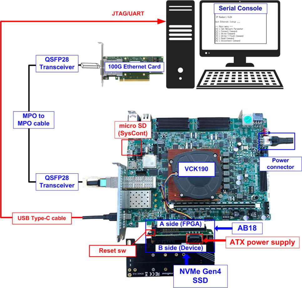
Figure 1 FTP Server by muNVMe-IP (Gen4) on VCK190
2 FPGA Setup
This section provides detailed instructions for preparing the FPGA board to run FTP Server by muNVMe-IP (Gen4).
1) Connect USB cables between FPGA board and PC for JTAG programming and Serial console. For VCK190 board, connect a USB type-C cable.
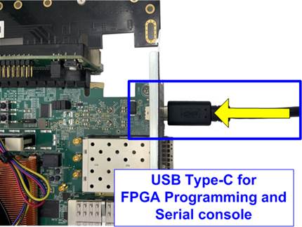
Figure 2 USB type-C cable connection
2) Connect the power adapter to the FPGA development board.
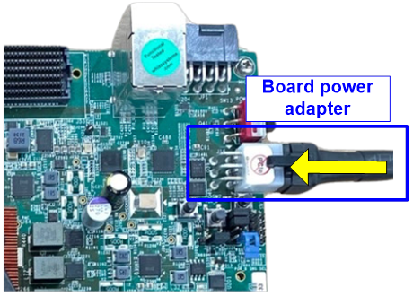
Figure 3 Connect power adapter to FPGA board
3) Connect the 100G Ethernet cable between FPGA board and PC. For VCK190, insert a 100G QSFP28 transceiver with MPO to MPO cable to the QSFP connector on FPGA board, as shown in Figure 4.
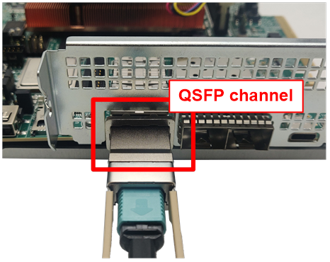
Figure 4 100G Ethernet Connection by QSFP28 transceiver and MPO to MPO cable
4) Insert the other end of the MPO cable which connects to QSFP28 transceiver into the 100G Ethernet card on the PC.
5) Set up and connect the NVMe Gen4 SSD to the PCIe adapter board. In this document, the AB18 is used by following these steps.
i) Ensure that two mini jumpers are inserted at J5 connector on AB18.
ii) Connect ATX power supply to AB board.
iii) Connect PCIe connector on FPGA board to FPGA Side (A-side) of the AB board, and connect the NVMe PCIe SSD to the device side (B-Side) of the AB board, as shown in Figure 5.
Warning: Ensure that the SSD is correctly inserted into the B-side of the AB18 (not the A-side) before powering on the system
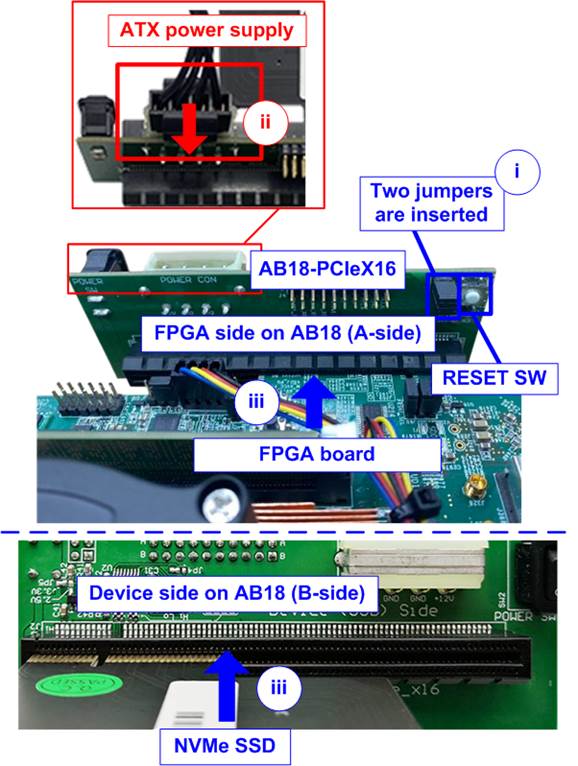
Figure 5 Setup AB18-PCIeX16 connection
6) Power on PCIe adapter board.
7) Power on the FPGA board.
For VCK190 board, ensure that it boots from the SD card to launch the BEAM tool. Booting with a configuration other than the BEAM tool may cause issues with the clock programming functionality in the Board User Interface, which is required in a later step. Follow these steps to boot the VCK190 board to launch the BEAM tool.
i) Ensure the SD card contains the Linux Prebuilt images for the VCK190, officially released by AMD Xilinx, available at https://xilinx-wiki.atlassian.net/wiki/spaces/A/pages/18842316/Linux+Prebuilt+Images
If the SD card does not have the correct image, update it by following the guidance in the section “Installing the System Controller Image” in UG1573: https://docs.amd.com/r/en-US/VCK190/VMK180-Board-Evaluation-and-Management-BEAM-Tool-User-Guide-UG1573/Installing-the-System-Controller-Image
ii) Insert the micro SD card into the system controller’s SD card socket (J206) and set the DIP switch (SW11) to ON OFF OFF OFF to boot from the SysCont SD, as shown in Figure 6.
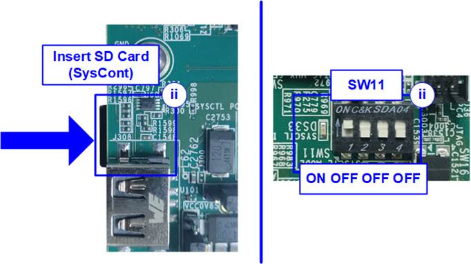
Figure 6 SD Card Boot Setting on VCK190
iii) Connect the VCK190 board to the PC using a USB cable. The PC should recognize three USB Serial Ports. Use the third port to monitor the board’s boot-up message.
iv) Open a Serial console and connect to the third USB Serial port with the following settings: Baud rate=115,200, Data=8-bit, Parity=None, and Stop bits=1-bit.
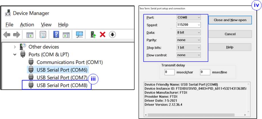
Figure 7 Serial Console Setting for VCK190
v) Power on the FPGA board and monitor the boot-up message in the console. Upon board boot-up completion, close this console to avoid port collision in future steps.
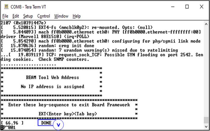
Figure 8 Boot-up Completion Message for VCK190
8) Configure the programmable clock for the FPGA board. If the board already uses the desired clock frequency, no further configuration is required. For the VCK190, use “VCK190 – Board User Interface” application to set the programmable clock to 322.265625 MHz, as shown in Figure 9.
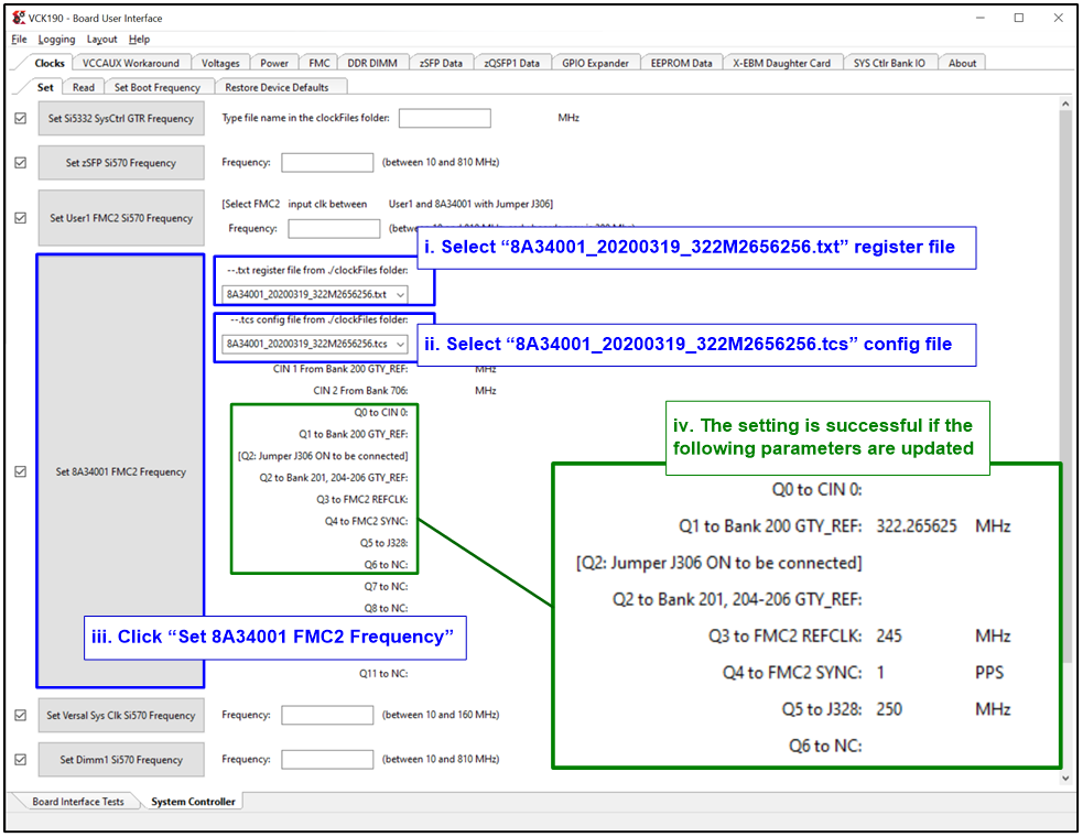
Figure 9 Reference Clock Programming for VCK190
9) Open Serial console. For the VCK190, select the lowest number of the newly detected COM ports. Use the same baud rate and data format settings as used previously for monitoring boot-up message.
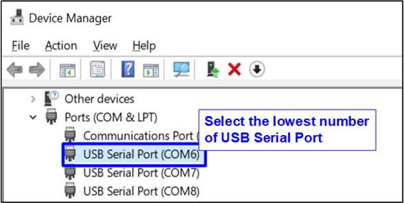
Figure 10 Serial Console for running the demo on VCK190
10) Open the Vivado TCL Shell to download the configuration file and firmware. Navigate to the download directory containing the ‘.bat’ file, ‘.pdi’ file, and ‘.elf’ file, and execute the ‘.bat’ file.
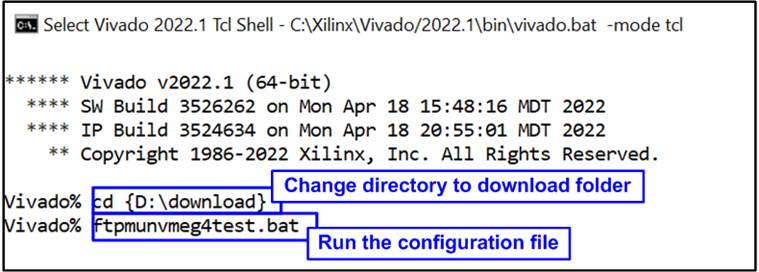
Figure 11 Download demo file on Vivado TCL shell by script file
11) On the Serial console, the main menu for testing the FTP Server demo will be displayed, awaiting user input.
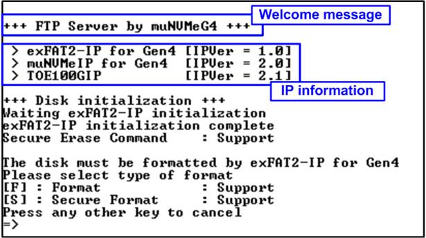
Figure 12 Serial console after successful configuration and firmware download
3 Revision History
|
Revision |
Date (D-M-Y) |
Description |
|
1.00 |
8-Nov-24 |
Initial version release |