FPGA set up for NVMeTCP25G-IP
Rev1.0 21-Aug-23
1 Introduction
This document describes how to setup FPGA board and test environment for running NVMeTCP25G-IP demo. The user can setup the test environment for accessing target NVMe SSD on Test PC across 25Gb Ethernet as shown in Figure 1‑1.
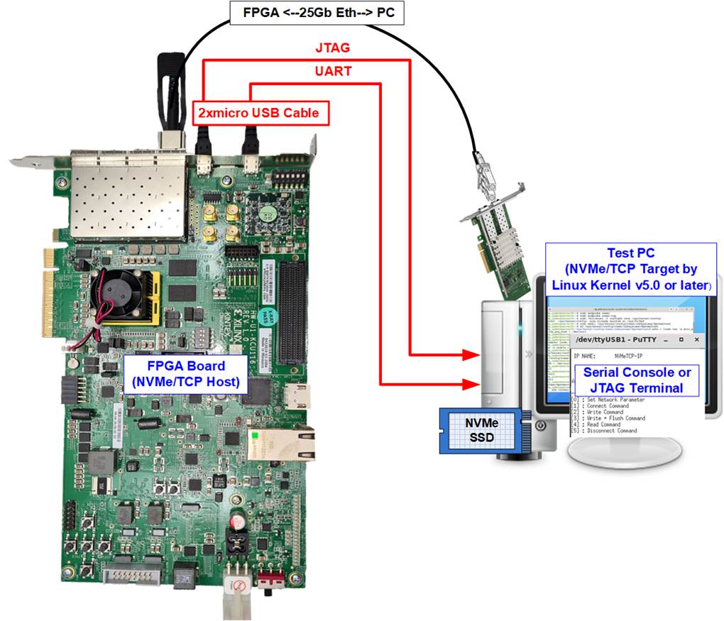
Figure 1‑1 Test environment for running the demo
Before running the test, please prepare following test environment.
- FPGA development boards: KCU116 or FB2CGHH@KU15P card
- Test PC
i) Install Linux kernel version 5.0 or later.
ii) Plug in with one NVMe SSD.
iii) Plug in with 25 Gigabit Ethernet card.
- 25 Gb Ethernet cable:
a) KCU116: 25 Gb SFP28 Active Optical Cable (AOC) or 25 Gb SFP28 transceivers (25G BASE-R) with optical cable (LC to LC, Multimode)
b) FB2CGHH@KU15P card: QSFP28 to 4xSFP28 cable
- Board power
a) KCU116: Power adapter of Xilinx board
b) FB2CGHH@KU15P card: Power by PCIe connector. It is able to use AB18-PCIeX16 board provided by Design Gateway with ATX power supply. More details of AB18 card are displayed on following website.
https://dgway.com/ABseries_E.html
- USB cable for connecting between FPGA and PC
a) KCU116: 2 micro USB cables for programming FPGA and Serial console
b) FB2CGHH@KU15P card: 1 mini USB cable for programming FPGA and JTAGUART
- User console
a) KCU116: Serial console software such as Putty installed on PC. The setting on the console is Baudrate=115,200, Data=8-bit, Non-parity, and Stop=1-bit.
b) FB2CGHH@KU15P card: JTAG Terminal
- Vivado tool for programming FPGA, installed on PC
Note: Example hardware for running the demo is listed as follows.
[1] 25G Network Adapter: Nvidia MCX631102AC-ADAT
[2] a) KCU116: 25G SFP28 Active Optical Cable: S28-AO01
https://www.fs.com/sg/products/68335.html
b) SFP28 to QSFP28 connection
SFP28 Transceiver: AZS85-S28-M1
https://www.sfpcables.com/25gb-s-sfp28-sr-transceiver-850nm-up-to-100m-2866
QSFP28 Transceiver: AMQ28-SR4-M1
https://www.sfpcables.com/100gb-s-qsfp28-sr4-optical-transceiver-module-1499
MTP to 4xLC Fiber cable: OM4-MTP-8LC-1M
https://www.fs.com/products/68047.html
[3] Test PC:
Motherboard : Gigabyte Z590 AORUS MASTER (rev. 1.0)
CPU : Intel i7-11700K CPU 3.6 GHz
RAM : 32 GB DDR4
OS : LinuxOS with kernel version 5.4.0-81
[4] Target NVMe SSD: 1 TB WD 850SN
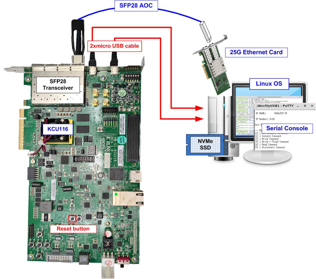
Figure 1‑2 NVMeTCP25G-IP demo on KCU116
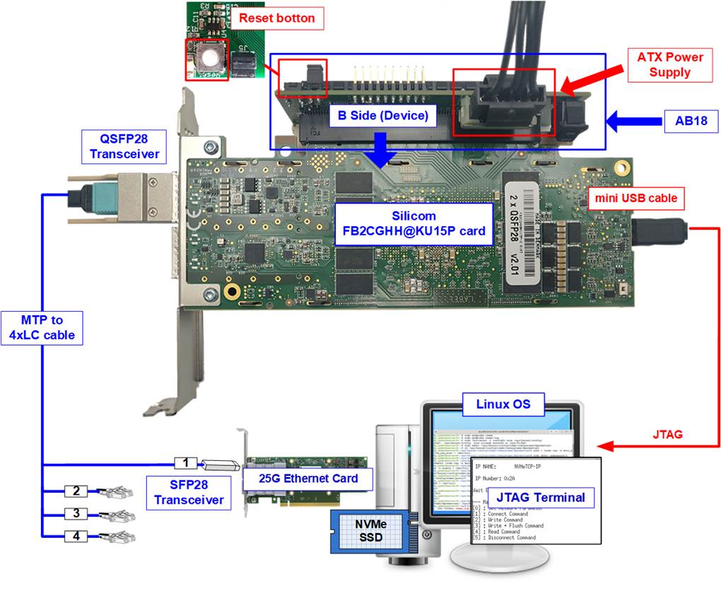
Figure 1‑3 NVMeTCP25G-IP demo on FB2CGHH@KU15P
2 FPGA setup
This topic describes the details to set up FPGA board for running the demo.
1) Connect USB cables between FPGA and PC for JTAG programming and Serial console/JTAGUART.
a) KCU116 board: Connect two micro USB cables
b) FB2CGHH@KU15P card: Connect one mini USB cable
2) Connect power supply to FPGA development board/FPGA accelerator card.
a) KCU116 board: Connect Xilinx power adapter
b) FB2CGHH@KU15P card: Connect the card to PC or AB18-PCIeX16 board by following step
i) Confirm that two mini jumpers are inserted at J5 connector on AB18.
ii) Connect ATX power supply to AB board.
iii) Connect PCIe connector on FPGA board to Device Side (B-Side), as shown in Figure 2‑1.
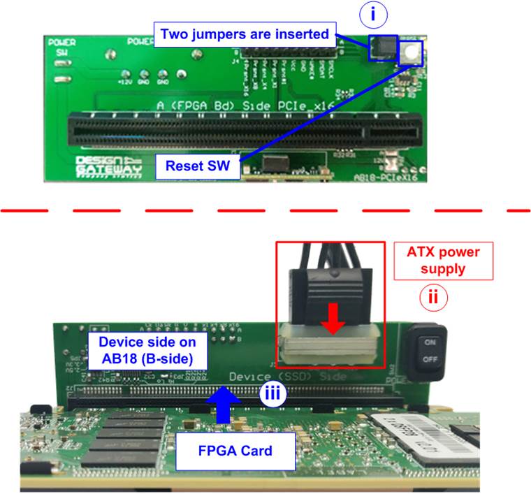
Figure 2‑1 AB18-PCIeX16 connection for power supply of FB2CGHH@KU15P card
3) Connect 25Gb Ethernet cable between FPGA board and PC.
a) KCU116: Insert 25G SFP28 AOC cable between FPGA board (on the left-most channel) and 25Gb Ethernet card on Test PC, as shown in Figure 2‑2.
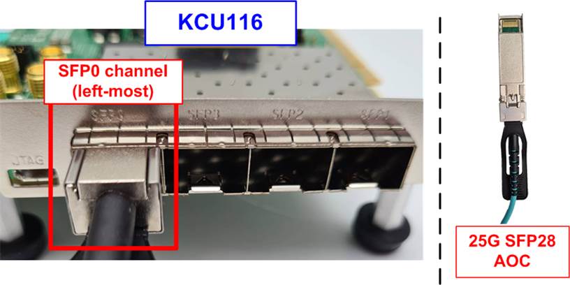
Figure 2‑2 25Gb connection on KCU116 board by 25G SFP28 AOC
b) FB2CGHH@KU15P: Insert QSFP28 to SFP28 cable by using QSFP1 connector on FPGA and plug SFP28 no.1 to 25Gb Ethernet card on Test PC, as shown in Figure 2‑3
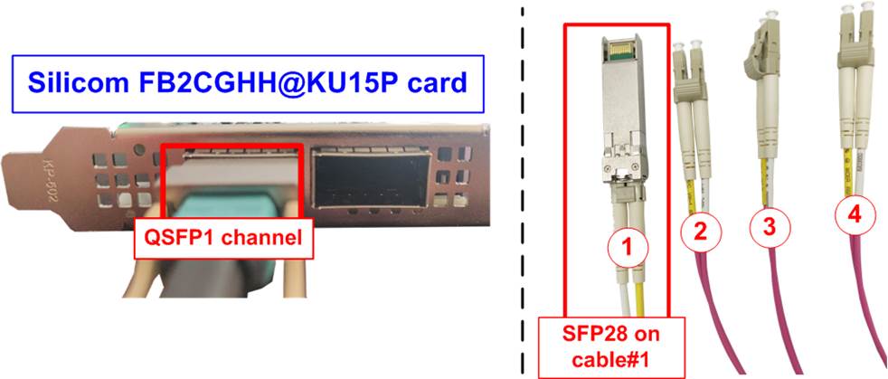
Figure 2‑3 25Gb connection on FB2CGHH@KU15P card
4) Power on FPGA board.
5) Only KCU116, set programmable clock on FPGA board to 322.265625 MHz
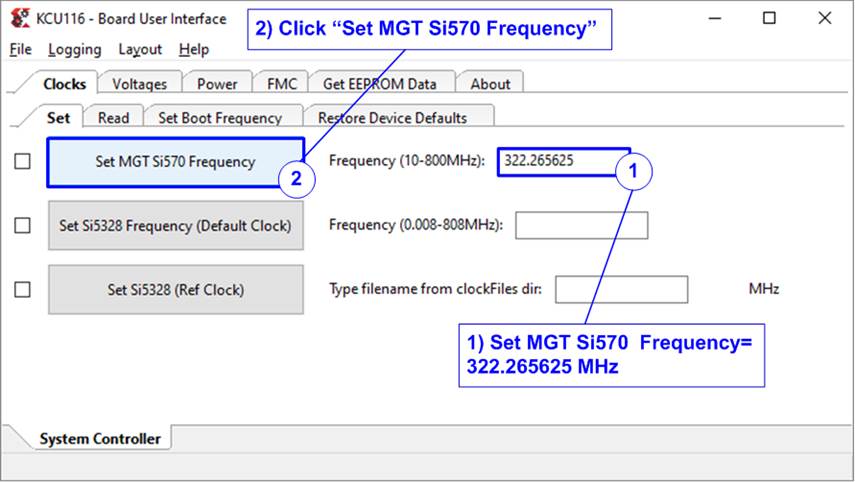
Figure 2‑4 Reference clock programming for KCU116
3 PC setup
The step describes the console setting and FPGA programmer tools on PC for running the demo. Both Windows OS and Linux OS are displayed.
3.1 KCU116 board
3.1.1 Serial console
When connecting FPGA board to PC, many COM ports from FPGA connection are detected and displayed. Please select the correct COM port for running the demo.
Serial console setting: Baud rate=115,200, Data=8-bit, Non-Parity and Stop = 1-bit.
Windows OS
Select Standard COM port.
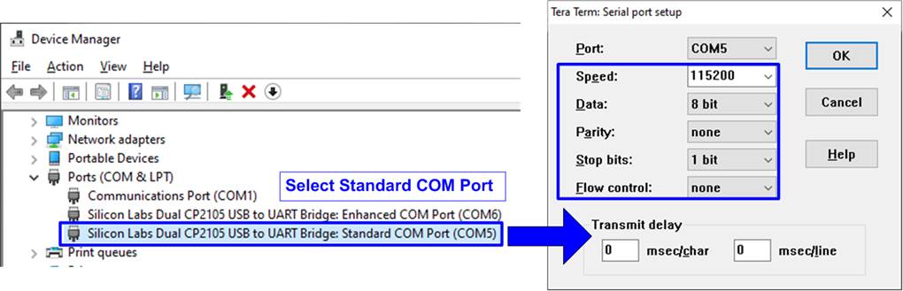
Figure 3‑1 COM port number for Serial console on Windows OS
Linux OS
When connecting FPGA board to PC, many USB Serial ports from FPGA connection are detected and displayed, as shown in Figure 3‑2.
Use following command to list USB Serial ports.
>> dmesg | grep ttyUSB
Select the second port.

Figure 3‑2 Command to scan USB Serial ports on Linux OS
Figure 3‑3 shows the example to configure Serial by using Putty application. Serial console setting: Baud rate=115,200, Data=8-bit, Non-Parity and Stop = 1.
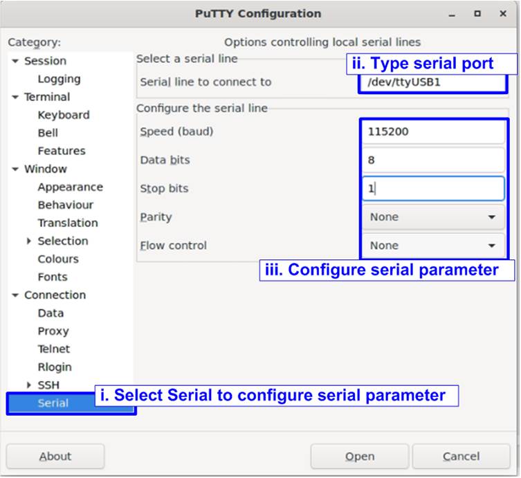
Figure 3‑3 Serial console setting on Linux OS
3.1.2 FPGA configuration
This topic shows how to load configuration file of the demo to FPGA board.
Open Vivado tools and program bit file by using Hardware manager, as shown in Figure 3‑4.
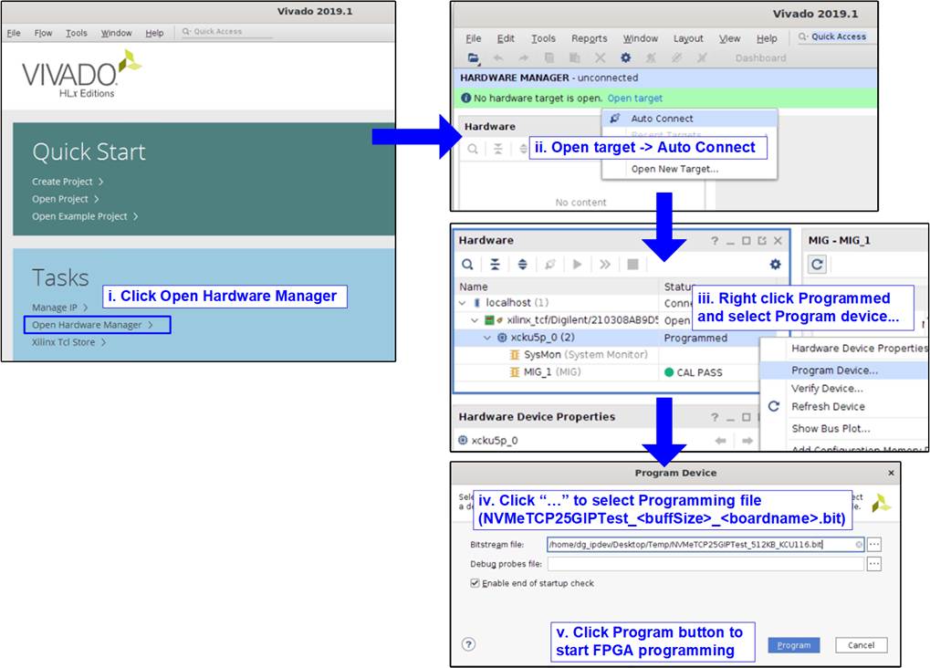
Figure 3‑4 KCU116 Configuration
3.2 FB2CGHH@KU15P card
Open vivado TCL shell and browse to the directory that includes batch file, bit file, and elf file of the demo. After that, run the test by typing following command
i) >> nvmetcpiptest_Silicom.bat
Note: This step is to download configuration file and firmware, as shown in Figure 3‑5
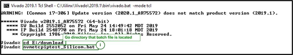
Figure 3‑5 Command script to download demo file on Vivado TCL shel
ii) >> xsdb.bat
iii) >> connect -url tcp:127.0.0.1:3121
iv) >> targets -set -filter {name =~"*Debug*"}
v) >> jtagterminal -start
vi) >> con
Note: Above steps are to connect JTAGUART module and run JTAG terminal to be user console, as shown in Figure 3‑6
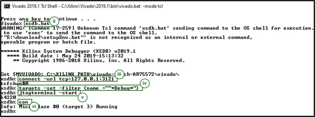
Figure 3‑6 Open JTAG Terminal
4 Welcome message
After finishing FPGA configuration, welcome message is displayed on FPGA console (Serial console or JTAG Terminal) as shown in Figure 4‑1.
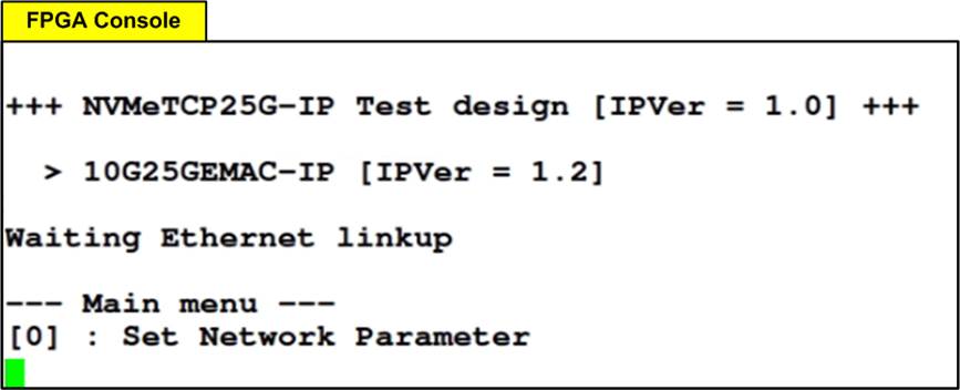
Figure 4‑1 Welcome screen
5 Revision History
|
Revision |
Date |
Description |
|
1.0 |
25-Mar-21 |
Initial version release |