FPGA Set up for NVMe-IP for Gen5 Demo
This document outlines the steps required to configure an FPGA and set up the environment for running the NVMe IP for Gen5 series demo with NVMe SSDs on an FPGA development board. These demos allow direct access to NVMe SSD via a PCIe adapter board, with test operations controlled by a Serial console.
1 Environment Requirement
To successfully run the demo on the FPGA development board, ensure the following components are prepared.
1) Supported FPGA Development boards: VHK158 and VPK120
2) A PC installing FPGA programmer software (Vivado) and Serial console software such as HyperTerminal or TeraTerm
3) PCIe Gen5 adapter boards provided by Design Gateway: AB19-M2PCI and AB20-U2PCI
https://dgway.com/ABseries_E.html
4) A power adapter for the FPGA board
5) An ATX power supply for the PCIe adapter board
6) An NVMe Gen5 SSD connected to the PCIe adapter board
7) USB cable for JTAG programming and Serial console.
· VHK158 : One USB Type-C cable
· VPK120 : One micro-USB cable
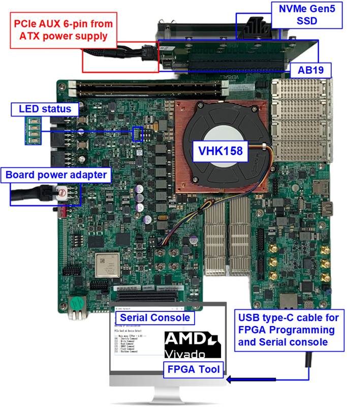
Figure 1 NVMe-IP for Gen5 Demo Setup on VHK158 with AB19
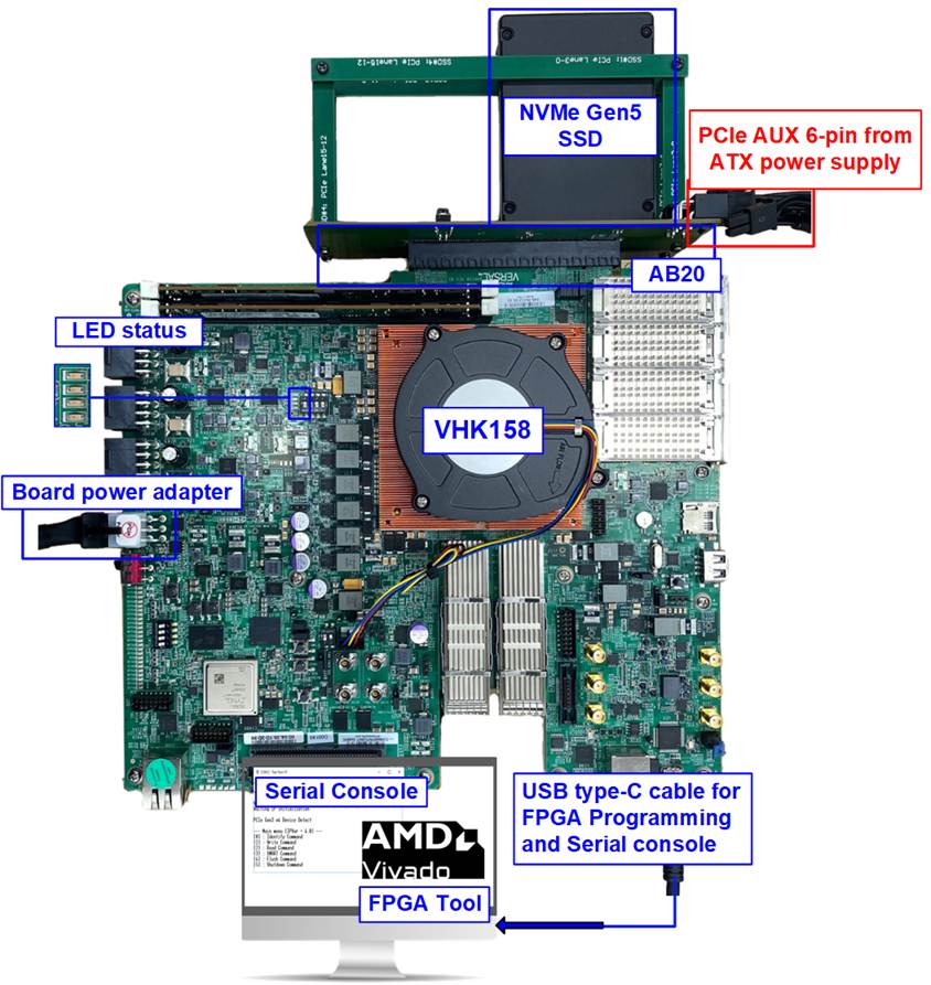
Figure 2 NVMe-IP for Gen5 Demo Setup on VHK158 with AB20
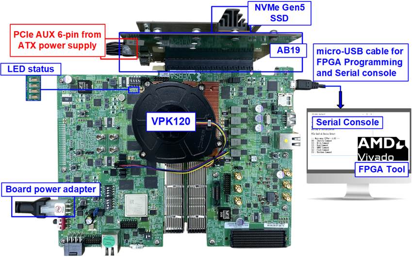
Figure 3 NVMe-IP for Gen5 Demo Setup on VPK120 with AB19
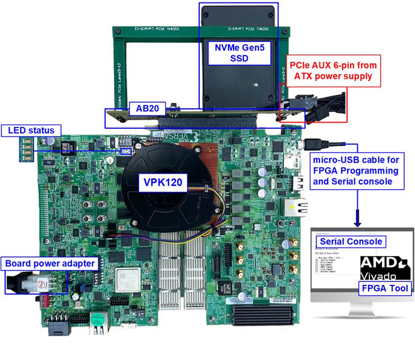
Figure 4 NVMe-IP for Gen5 Demo Setup on VPK120 with AB20
2 Demo Setup
2.1 Board Setup
Follow these steps to set up the board for the demo.
1) Power off the system.
2) Check the DIP switch settings for JTAG configuration. For VHK158/VPK120, set SW1=all ON and SW3[1:0]=OFF, ON.
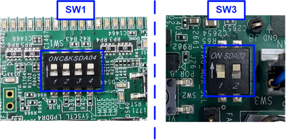
Figure 5 Setting DIP Switch on FPGA Board
3) Connect PCIe Gen5 adapter, NVMe SSD, and FPGA board by following these steps.
AB19-M2PCI
i) Ensure that the two mini jumpers at JP1 on AB19 are inserted between pins 1-3 and 2-4.
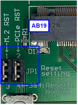
Figure 6 Check Jumpers on AB19
ii) Connect the NVMe SSD to CN2: PCIe Lane 7-4 on AB19 board, as shown in Figure 7.
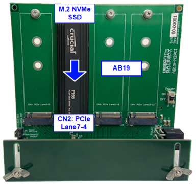
Figure 7 Connect NVMe SSD to CN2 of AB19
iii) Connect the 6-pin PCIe AUX cable from the ATX power supply to the AB19-M2PCI board, as shown in Figure 8.
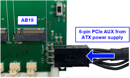
Figure 8 Connect 6-Pin PCIe Power Supply to AB19
iv) Insert the AB19 into the PCIe connector on the FPGA board.
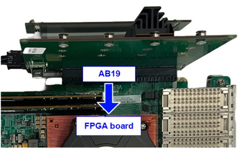
Figure 9 Connect AB19 to FPGA Board
v) Adjust the height of the AB19 by sliding the support board up or down until the AB19 is aligned with the PCIe connector on the FPGA board. Once aligned, tighten the wing nut to fix the height.
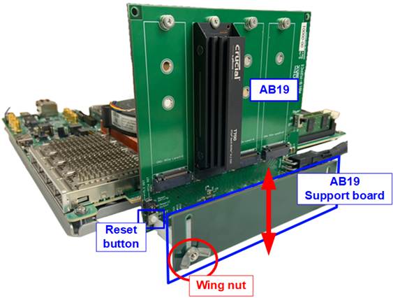
Figure 10 Adjust the Height of AB19 Support Board
AB20-U2PCI
i) Ensure that the two mini jumpers at JP1 on AB20 are inserted between pins 1-4 and 2-3.
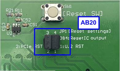
Figure 11 Check Jumpers on AB20
ii) Connect the NVMe SSD to CN2: PCIe Lane 7-4 on AB20 adapter board and connect the 6-pin PCIe AUX cable from the ATX power supply to the AB20-U2PCI board, as shown in Figure 12.
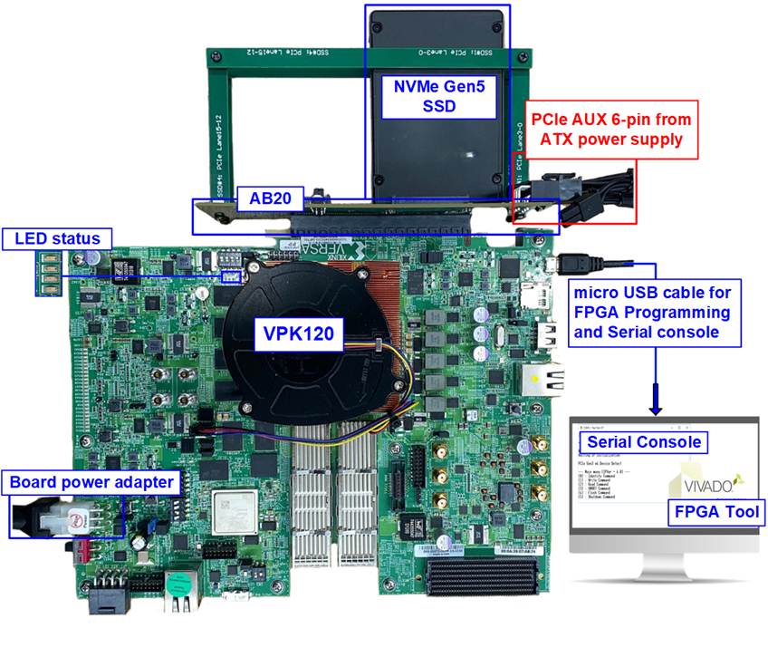
Figure 12 Connect NVMe SSD to CN2
of AB20 and Connect 6-Pin PCIe Power Supply to AB20
iii) Insert the AB20 into the PCIe connector on the FPGA board. Adjust the height of the FPGA board to align with the PCIe connector on the AB20-U2PCI adapter board.
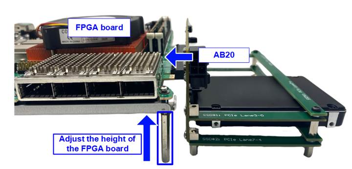
Figure 13 Connect AB20 to FPGA Board and Adjust Height of FPGA board
4) Connect the USB cable from the FPGA board to the PC for JTAG programming and Serial console.
· VHK158: Connect USB Type-C cable for both JTAG and Serial console.
· VPK120: Connect micro-USB cable for both JTAG and Serial console.
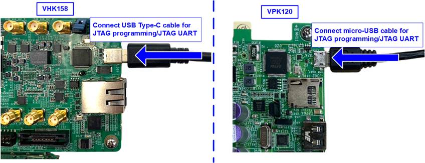
Figure 14 USB Type-C Cable Connection
5) Connect the power adapter to the FPGA board.
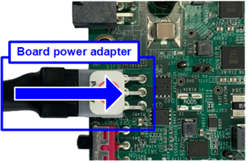
Figure 15 Connect Power Adapter to FPGA Board
2.2 File Programming
Follow these steps to program the demo file onto the FPGA board.
1) Connect the USB cable from the FPGA board to the PC. Three USB Serial Ports should be detected in the Device Manager. Open Serial console for monitoring the boot-up messages by selecting the third port. The console settings are 115200 speed, 8-bit data, no parity, 1-bit stop, and no flow control.
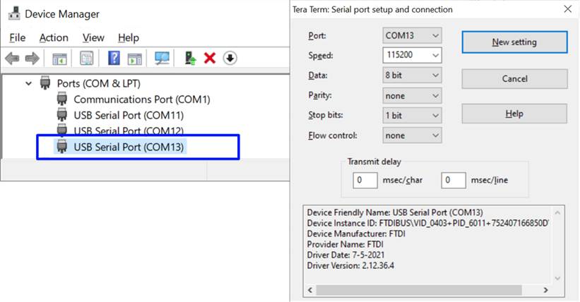
Figure 16 Serial Console for Boot-Up
2) Turn on the power to the FPGA board, PCIe adapter board, and the ATX power supply.
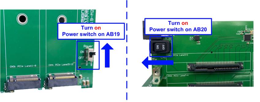
Figure 17 Turn On Power Switch on Adapter Board
3) Wait until the boot message on the console is completed.
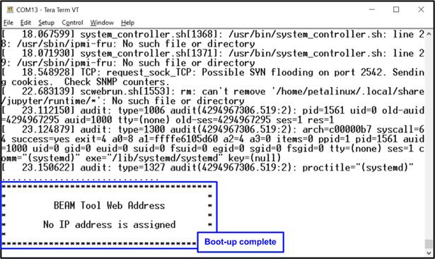
Figure 18 Boot-Up Message of Power-On Sequence
4) Close the current Serial console and open a new one for running the demo by selecting the first port. The configuration for speed and data format is similar to the previous console.
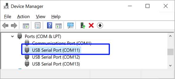
Figure 19 Serial Console for Running the Demo
5) Open the Vivado TCL Shell to download the configuration file and firmware. Browse to the download directory containing the ‘.bat’ file, ‘.pdi’ file, and ‘.elf’ file, then execute the ‘.bat’ file.
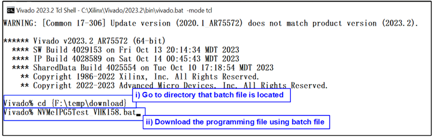
Figure 20 Download Demo File on Vivado TCL Shell by Script File
6) Check the LED status on the FPGA board. During the PCIe initialization process, both LED[0] and LED[1] should be ON. Once the NVMe-IP completes initialization, LED[1] will turn OFF, as shown in Figure 21. Additional LED descriptions are provided in Table 1.
Table 1 LED Definition
|
GPIO LED |
ON |
OFF |
|
0 |
Reset sequence is completed |
Reset sequence incompletes |
|
1 |
NVMe-IP is busy |
NVMe-IP is idle |
|
2 |
NVMe-IP detected an error |
NVMe-IP has no error |
|
3 |
Data verification failed |
Data verification passed |
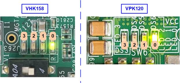
Figure 21 LED Status After Loading Configuration File and Completing Initialization
7) On the Serial console, the main menu for testing the NVMe-IP will be displayed, waiting for user input.
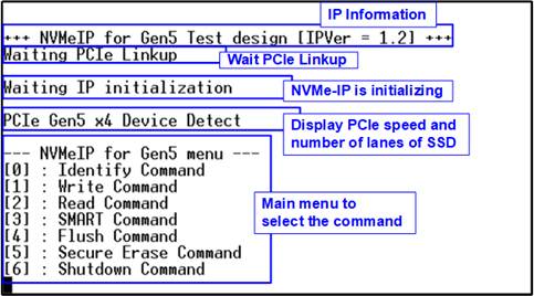
Figure 22 Main Menu After Completing IP Initialization
3 Revision History
|
Revision |
Date (D-M-Y) |
Description |
|
1.01 |
16-Dec-25 |
Support VPK120 and AB20-U2PCI |
|
1.00 |
15-Aug-24 |
Initial version release |