FPGA setup for 2-Ch RAID0 by NVMe-IP Demo
Rev2.2 3-Jul-23
This document describes the FPGA and test environment setup for running 2-ch RAID0 by using NVMe-IP, NVMeG3-IP, NVMeG4-IP, or NVMe-IP for Gen4 demo on FPGA development board by using the AB17-M2FMC board or AB18-PCIeX16 board with Quad M.2 card for connecting with two M.2 NVMe SSDs. It is recommended to use the same SSD models for RAID0 operation to match SSD characteristic. User controls test operation via Serial console.
1 Test Environment setup
To run the demo on FPGA development board, please prepare following environment.
1) FPGA development board: VCK190, VCU118, ZCU106, ZCU102, KCU105
2) The adapter of M.2 SSD
a. AB17-M2FMC board
https://dgway.com/ABseries_E.html
b. AB18-PCIeX16 board with Quad M.2 card
https://dgway.com/ABseries_E.html
https://www.asrock.com/mb/spec/product.asp?Model=ULTRA%20QUAD%20M.2%20CARD
3) Two M.2 NVMe SSDs, inserting to M.2 connector on AB17/Quad M.2 card
4) For AB18 only, ATX power supply for PCIe adapter board
5) Xilinx power adapter for FPGA board
6) Two micro USB cables/one USB type-C cable for programming FPGA and Serial console, connecting between FPGA board and PC
7) PC installing Xilinx programmer software (Vivado) and Serial console software such as TeraTerm and HyperTerminal
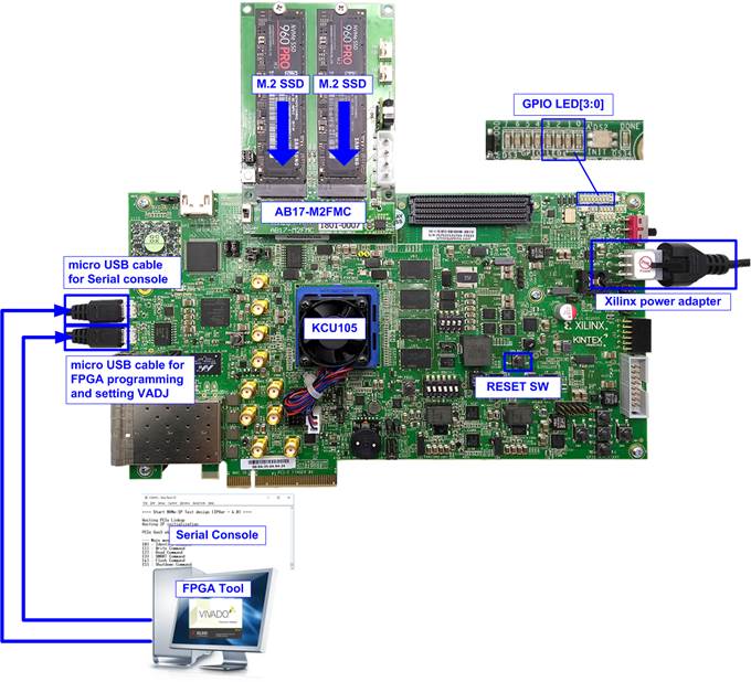
Figure 1‑1 NVMe RAID0x2 demo setup by AB17 on KCU105

Figure 1‑2 NVMe RAID0x2 demo setup by AB17 on ZCU106

Figure 1‑3 NVMe RAID0x2 demo setup by AB17 on ZCU102

Figure 1‑4 NVMe RAID0x2 demo setup by AB18 on VCU118

Figure 1‑5 NVMe RAID0x2 demo setup by AB17 on VCK190
2 FPGA board connection setup
1) Power off system.
2) Connect two M.2 NVMe SSDs to AB17-M2FMC/Quad M.2 card
a) For AB17, connect two M.2 NVMe SSDs to Drive#1 and #2 connector and then connect AB17-M2FMC to HPC on KCU105 (J22), HPC-1 on ZCU106 (J5), HPC-0 on ZCU102 (J4), or FMCP-1 on VCK190 (J51) as shown in Figure 2‑1.
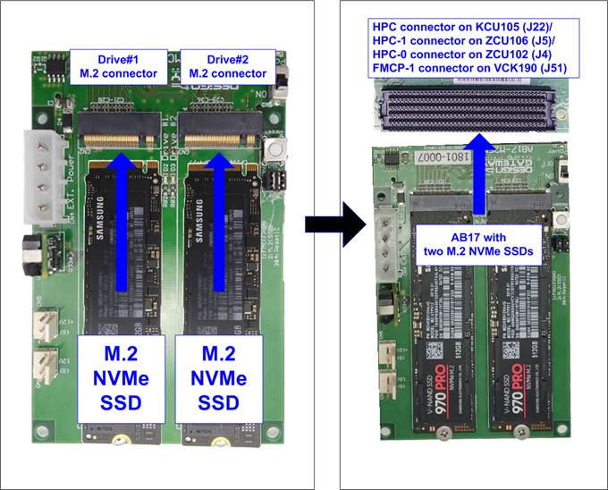
Figure 2‑1 Connect M.2 NVMe SSDs to AB17-M2FMC
b) For Quad M.2 card, please follow below steps.
i. Insert two M.2 NVMe SSDs to M2_1 and M2_2 connectors on Hyper Quad M.2 card, as shown in Figure 2‑2.

Figure 2‑2 Two M.2 NVMe SSDs on Hyper Quad M.2 Card
ii. Confirm that two mini jumpers are inserted at J5 connector on AB18. After that, connect FPGA Side (A-side) on AB18 to PCIe connector on FPGA board and connect Hyper Quad M.2 NVMe SSD Card to device side (B-Side) on AB18, as shown in Figure 2‑3.
Warning: Please confirm that the Hyper Quad M.2 Card is inserted in the correct side of AB18 (B-side, not A-side) before power on system.
iii. Connect ATX power supply to AB18-PCIeX16 board.

Figure 2‑3 AB18, Quad M.2 Card, and FPGA board connection
3) Connect USB cable between FPGA board and PC for FPGA programming and Serial console as shown in Figure 2‑4
a) VCK190: Connect one USB type-C cable.
b) Other boards: Connect two micro USB cables.
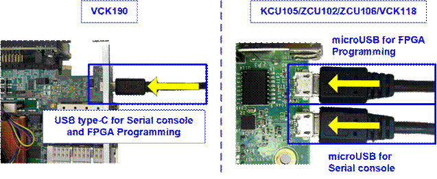
Figure 2‑4 USB cable connection
4) Turn on power switch of AB17/AB18, ATX power supply for AB18 (when using AB18), and FPGA development board as shown in Figure 2‑5.
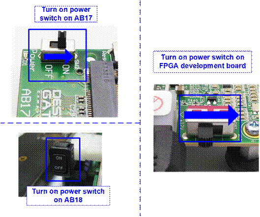
Figure 2‑5 Turn on power
5) After connecting USB cables to PC, many COM ports are detected.
a) KCU105/VCU118: Select Standard COM port
b) ZCU106/ZCU102/VCK190: Select the lowest number of the additional COM ports.

Figure 2‑6 Additional COM port when USB cable is plugged-in
On Serial console, the setting is as follows.
Set Buad rate=115,200, Data=8-bit, Non-Parity, and Stop = 1, as shown in Figure 2‑7.
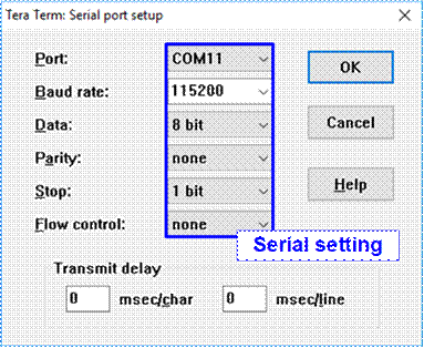
Figure 2‑7 Serial console setting
6) For KCU105 board by AB17, open Serial console to connect with Enhanced COM port (Buad rate=115,200 Data=8 bit Non-Parity Stop=1). The console shows System Controller menu, as shown in Figure 2‑8. To set VADJ of FMC to 1.8V, the following step is recommended.
i. Input ‘4’ to select Adjust FMC Settings.
ii. Input ‘4’ to set FMC VADJ to 1.8V.
iii. Input ‘0’ to return to Main Menu.
iv. Input ‘2’ to get PMBUS Voltages.
v. Input ‘7’ to get VADJ1V8 Voltage. The output voltage of this menu must be equal to 1.8V to confirm that VADJ has been set completely.
For more details of System Controller, please check “UG917 KCU105 Board User Guide” in section “Appendix C: System Controller”.
https://www.xilinx.com/support/documentation/boards_and_kits/kcu105/ug917-kcu105-eval-bd.pdf

Figure 2‑8 Setting VADJ on FMC for KCU105
7) Program configuration file to FPGA board.
KCU105 and VCU118 board
Open Vivado tool to download configuration file, as shown in Figure 2‑9.
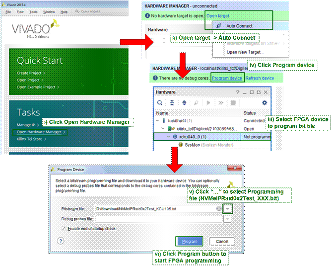
Figure 2‑9 Programmed by Vivado on KCU105/VCU118
ZCU102, ZCU106, and VCK190 board
Open Vivado TCL shell and change directory to download or directory that batch file is located. Next, type “NVMeXXRaid0x2Test_ZCU106/ZCU102/VCK190.bat”, as shown in Figure 2‑10.

Figure 2‑10 Command script to download demo file on Vivado TCL shell
8) Check LED status on FPGA board. The description of LED is as follows.
Table 2‑1 LED Definition
|
GPIO LED |
ON |
OFF |
|
0 |
Normal operation |
1) PCIe Clock or system Clock is not locked. 2) Reset button is pressed. |
|
1 |
System is busy |
Idle status |
|
2 |
IP Error detect |
Normal operation |
|
3 |
Data verification fail |
Normal operation |
9) After programming completely, LED[0] and LED[1] turn ON until finishing PCIe initialization process. After that, LED[1] changes to OFF when PCIe completes initialization process.
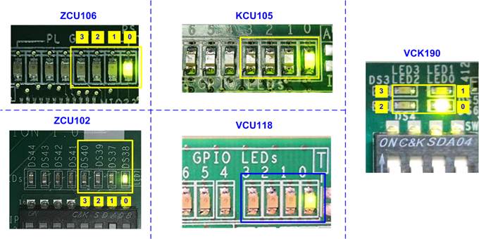
Figure 2‑11 LED status after finishing PCIe initialization
10) Main menu is displayed in Serial console and ready to receive command.
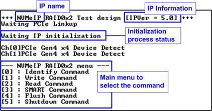
Figure 2‑12 Main menu after RAID0 finishes initialization
3 Revision History
|
Revision |
Date |
Description |
|
2.2 |
3-Aug-22 |
Include NVMe-IP for Gen4 and support VCK190 board |
|
2.1 |
15-Jul-21 |
Include NVMeG4-IP demo |
|
2.0 |
29-Jun-20 |
Remove demo instruction from the document and add NVMeG3-IP |
|
1.0 |
9-Oct-17 |
Initial version release |