SATA IP Transport & Link Layer Core Data Sheet

Core Facts |
|
|
Provided with Core |
|
|
Documentation |
User Guide, Design Guide |
|
Design File Formats |
Encrypted File |
|
Instantiation Templates |
VHDL |
|
Reference Designs & Application Notes |
Quartus Project, See Reference Design Manual |
|
Additional Items |
Demo on CycloneV SX SoC/ArriaV GX/ ArriaV ST SoC/StratixV GX/ Arria10 SoC development kit/ Arria10 GX development kit |
|
Support |
|
|
Support Provided by Design Gateway Co., Ltd. |
|
Design Gateway Co.,Ltd
E-mail: ip-sales@design-gateway.com
URL: design-gateway.com
Features
· Compliant with the Serial ATA specification revision 3.0
· Support both SATA Host and SATA Device
· Simple user interface and 32-bit data bus
· Include two 4KB FIFOs to be data buffer
· RX Elastic buffer to interface PHY
· Support SATA-III (ArriaV GX/StratixV GX/ArriaV ST/Arria10 SoC/Arria10 GX) or SATA-II Speed (CycloneV SX SoC) and NCQ command
· Require low user clock frequency (at least 150 MHz for SATA-III or 75 MHz for SATA-II)
· CONT primitive support for continue primitive suppression to reduce EMI
· Support 40bit width PHY implemented by Transceiver Block
· Many reference designs on Altera evaluation board running with AB11-HSMCSATA, AB12-HSMCRAID, or AB09-FMCRAID adapter board from Design Gateway
- 1-ch SATA host demo reference design
- 4-ch SATA RAID0 demo reference design
- 1-ch SATA host with exFAT support design
- SATA AHCI IP demo reference design with Linux OS
- 1-ch SATA host demo by SATA HCTL IP
- 4-ch SATA RAID0 demo by SATA Host IP
Table 1: Example Implementation Statistics
|
Family |
Example Device |
Fmax (MHz) |
ALMs |
Registers1 |
Pin2 |
Block Memory bit |
Transceiver3 |
Design Tools |
|
CycloneV SX |
5CSXFC6D6F31C6 |
250 |
668 |
1,135 |
194 |
33,792 |
1 |
QuartusII 15.1 |
|
ArriaV GX |
5AGXFB3H4F35C4 |
263 |
691 |
1,129 |
194 |
33,792 |
1 |
QuartusII 15.1 |
|
ArriaV ST |
5ASTFD5K3F40I3 |
263 |
688 |
1,145 |
194 |
33,792 |
1 |
QuartusII 15.1 |
|
StratixV GX |
5SGXEA7K2F40C2 |
450 |
678 |
1,129 |
194 |
33,792 |
1 |
QuartusII 14.0 |
|
Arria10 SX |
10AS066N3F40E2SGE2 |
500 |
684 |
1106 |
194 |
33,792 |
1 |
QuartusII 15.1 |
Notes:
1) Actual logic resource dependent on percentage of unrelated logic
2) Assuming all core I/Os and clocks are routed off-chip
3) Transceiver is not used in SATA IP core, but they are used in SATA PHY design.
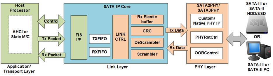
Figure 1: SATA IP Block Diagram
Applications
SATA IP Core is ideal for use in a variety of storage application such as embedded storage system and High speed with large capacity data acquisition system. System performance, device capacity, and data reliability are increased by using multiple SATA IPs as RAID0 operation. SATA IP is the solution which achieves high speed performance, scalability, and features extensibility.
The IP supports both Host and Device mode, so it can be applicable for Secure storage.
General Description
Free demo sof file to evaluate SATA IP on many Altera evluation boards are provided on the website. Besides, various reference designs are provided to fit with many SATA applications such as 1-ch Host reference design and 4-ch RAID0 design. RAID0 is the solution to increase transfer performance and device capacity by connecting multiple SATA devices to the same Host.
Furthermore, four optional IPs are additional topped-up to complete the SATA solution, i.e., HCTL IP, AHCI IP, FAT32 IP, and exFAT IP. More information can be found on our website.
https://dgway.com/SATA-IP_A_E.html
Functional Description
SATA IP converts SATA FIS packet sent by Processor/UserLogic to be data stream for SATA PHY layer. SATA IP implements the logic for operating Link layer and Transport layer. Two asynchronous FIFOs are included to be the data buffer between Transport layer logic and Link layer logic which run in different clock domain. Also, FIFO is applied to be data flow control in SATA IP.
Link Layer
The Link layer is the middle layer between Transport layer and SATA PHY. It handles the primitives for interface with SATA PHY and the packet for interface with Transport layer.
· RX Elastic Buffer
This buffer is used to change clock domain of received data in PHY layer from recovery clock (RECCLK) to synchronous with core_clk.
· CRC
The CRC of a frame is a Dword (32-bit) field that shall follow the last Dword of the contents of a FIS and precede EOF primitive.
· Scramble
The content of a frame is scrambled before forwarding to SATA PHY. Scrambling is performed on Dword quantities by XORing the data to be transmitted with output of a linear feedback shift register (LFSR) by SATA IP.
· Descramble
The content of a frame from SATA PHY is descrambled before sending to Transport layer. Descrambling is performed the same ways as scrambling to get FIS.
Transport Layer
Transport layer constructs frame information structure (FIS) for transmission. On the other hand, it decomposes received frame information structures. It also notifies Link layer of the required data flow control and generate status signals for upper layer.
· FIS Interface
Provides the interface and data flow control for transmits and receive a transferred transaction with Application layer.
Processor/UserLogic
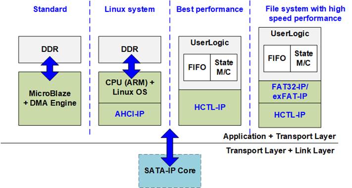
Figure 2: Processor/UserLogic implementation
In standard system, SATA IP operates with the host processor that runs the firmware for handling the packet with SATA IP. The SATA IP and the host proecessor include DMA Engine to handle FIS packet through main memory (DDR). This system is flexible to support various ATA commands and easy to upgrade the system specification. However, the system consumes large FPGA resources for building processor system and DDR controller.
As optional, AHCI IP, HCTL IP, FAT32 IP, and exFAT IP are purposed to complete Application layer of SATA protocol for many applications. AHCI IP is the option to integrate SATA IP to the processor system which runs OS and needs to access SATA IP by using standard driver, AHCI driver. While remaining IP cores are designed to minimize FPGA resource with high transfer performance achievement. They complete SATA host solutions without using the processor and DDR. The user interface of the IPs is very simple, so the user logic can be designed using simple state machine with some registers. HCTL IP implements SATA application layer which can fit to data acquisition system. FAT32 IP and exFAT IP are the additional solutions of HCTL IP to transfer data with SATA device by FAT32 and exFAT file system, not raw data format. Please see more details from our website.
https://dgway.com/SATA-IP_A_E.html
SATA PHY
SATA PHY design is designed by using Transceiver in V-series/10-series and this module has been proved on CycloneV SX SoC board/ArriaV GX Starter kit/StratixV GX board/ArriaV ST SoC/Arria10 SoC board/Arria10GX board at fixed SATA-II or SATA-III speed. The operation on user board or user design is not guaranteed. SATA PHY HDL source code is provided to customer after purchasing, so PHY parameter and operation can be modified by user.
Core I/O Signals
Descriptions of all I/O signals are provided in Table 2.
Table 2: Core I/O Signals
|
Signal |
Dir |
Clk |
Description |
|
Common Interface Signal |
|||
|
IPVersion[31:0] |
Out |
|
IP version number. |
|
trn_reset |
In |
trn_clk |
Reset SATA IP which is synchronous reset and active high. Assert at least 4 clock cycles of core_clk to reset SATA IP. |
|
trn_link_up |
Out |
trn_clk |
Transaction link up. Asserted when the core establishes the communication with SATA PHY. |
|
trn_clk |
In |
|
Clock signal for interface with the Host. This clock frequency must be higher than or requal to core_clk frequency. |
|
core_clk |
In |
|
Clock signal for interface with the SATA PHY, generated by SATA PHY. (150 MHz for SATA-III, 75 MHz for SATA-II). |
|
dev_host_n |
In |
trn_clk |
Device or Host design assignment. 0b: Host IP, 1b: Device IP (Use 0b for the host reference design) |
|
Transmit Transaction Interface |
|||
|
trn_tsof_n |
In |
trn_clk |
Not used now. |
|
trn_teof_n |
In |
trn_clk |
Transmit End-Of-Frame (EOF): Indicate end each SATA FIS packet. Active low. |
|
trn_td[31:0] |
In |
trn_clk |
Transmit Data: SATA FIS packet data to be transmitted. |
|
trn_tsrc_rdy_n |
In |
trn_clk |
Transmit Source Ready: Indicate that trn_td[31:0] from the Host is valid. Active low. |
|
trn_tdst_rdy_n |
Out |
trn_clk |
Transmit Destination Ready: Indicate that the core is ready to accept data on trn_td[31:0]. Active low. trn_tsrc_rdy_n must be de-asserted to 1b within 4 period of trn_clk after trn_tdst_rdy_n is de-asserted to 1b. Therefore, the core can accept 4 DWORD of trn_td[31:0] after trn_tdst_rdy_n is de-asserted to 1b. |
|
trn_tsrc_dsc_n |
In |
trn_clk |
Transmit Source Abort: Assert for 1 clock cycle of trn_clk during operation (between tsof and teof) when the user cancels current write operation. Active low. After asserting to 0b, the Core will send SYNC primitive to SATA PHY to abort the current transfer. The user needs to wait until trn_tdst_rdy_n ready again before sending the next packet. See Figure 5 for more details. |
|
trn_tdst_dsc_n |
Out |
trn_clk |
Transmit Destination Abort: Asserted for 1 clock cycle of trn_clk by the core to cancel current write operation when SYNC primitive is received. Active low. See Figure 7 for more details. |
|
Receive Transaction Interface |
|||
|
trn_rsof_n |
Out |
trn_clk |
Receive Start-Of-Frame (SOF): Indicate start each SATA FIS packet. Active low. |
|
trn_reof_n |
Out |
trn_clk |
Receive End-Of-Frame (EOF): Indicate end each SATA FIS packet. Active low. |
|
trn_rd[31:0] |
Out |
trn_clk |
Receive Data: SATA FIS packet data to be transmitted. |
|
trn_rsrc_rdy_n |
Out |
trn_clk |
Receive Source Ready: Indicate that trn_rd[31:0] from the core is valid. Active low. |
|
trn_rdst_rdy_n |
In |
trn_clk |
Receive Destination Ready: Indicate that the user is ready to accept data on trn_rd[31:0]. Active low. trn_rsrc_rdy_n will be de-asserted within 4 clock cycles of trn_clk after trn_rdst_rdy_n is de-asserted to 1b. Therefore, the user logic should support to accept 4 DWORD of trn_rd[31:0] after trn_rdst_rdy_n is de-asserted to 1b. |
|
trn_rsrc_dsc_n |
Out |
trn_clk |
Receive Source Abort: Assert 1 clock cycle of trn_clk by the core to cancel current read operation when SYNC primitive is received. Active low. See Figure 8 for more details. |
|
trn_rdst_dsc_n |
In |
trn_clk |
Receive Destination Abort: Assert 1 clock cycle of trn_clk during read operation (between rsof and reof) when the user cancels current read operation. Active low. After asserting this signal to 0b, the core sends SYNC primitive to SATA-PHY to abort the current transfer. The user needs to wait until trn_tdst_rdy_n ready again before sending the next packet. See Figure 6 for more details. |
|
Signal |
Dir |
Clk |
Description |
|
SATA PHY Interface |
|||
|
LINKUP |
In |
core_clk |
Indicate that SATA link communication is established. Active high. |
|
PLLLOCK |
In |
core_clk |
Indicate that PLL of SATA PHY is locked. Active high. |
|
TXDATA[31:0] |
Out |
core_clk |
32-bit transmitted data from the core to SATA PHY |
|
TXDATAK[3:0] |
Out |
core_clk |
4-bit Data/Control for the symbols of transmitted data. (0000b: data byte, 0001b: control byte, others: undefined). |
|
RECCLK |
In |
|
Clock Recovery to synchronous with received data from SATA PHY |
|
RXDATA[31:0] |
In |
RECCLK |
32-bit received data from the SATA PHY to the core. |
|
RXDATAK[3:0] |
In |
RECCLK |
4-bit Data/Control for the symbols of received data. (0000b: data byte, 0001b: control byte, others: undefined) |
|
RXDATAVALID |
In |
RECCLK |
Indicate that RXDATA from SATA PHY is valid. |
|
RXDATAOUT[31:0] |
Out |
core_clk |
RXDATA signal after Elastic buffer and synchronous with core_clk |
|
RXDATAKOUT[3:0] |
Out |
core_clk |
RXDATAK signal after Elastic buffer and synchronous with core_clk |
|
RXDATAVALIDOUT |
Out |
core_clk |
Indicate that RXDATAOUT is valid. |
Timing Diagram
As shown in Figure 3, data is transferred with asserting trn_tsrc_rdy_n to 0b after the core is ready (monitored by trn_tdst_rdy_n=0b). After trn_tdst_rdy_n is de-asserted to 1b, the core can receive more 4 data. trn_td and trn_tsrc_rdy_n are the signals used to write data and the valid of write data which are written to FIFO inside SATA IP. trn_teof_n and trn_tsrc_rdy_n are asserted to 0b when transferring the last data of the packet. After the packet is completely transferred to the core, the user waits until error code packet, generated by SATA IP, is received to show transfer status of a packet transaction.
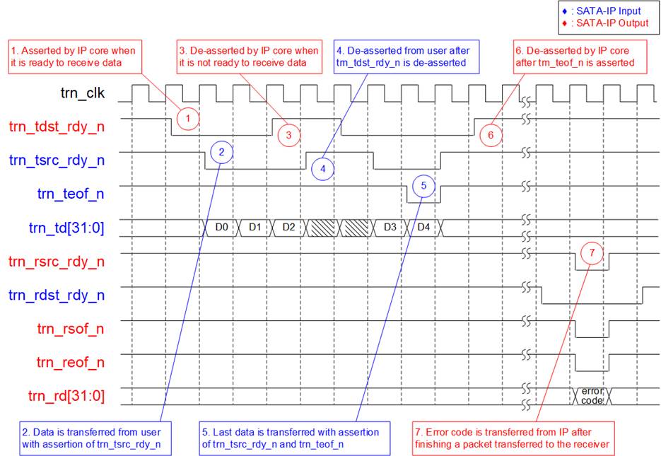
Figure 3: Transmit Transaction Interface Timing
Similar to Figure 3, the first data is transferred by the core after trn_rdst_rdy_n signal is asserted to 0b. trn_rdst_rdy_n signal must be de-asserted to 1b when free space of data buffer inside the user is less than 5 (Up to four data are transferred after de-asserting ready signal). After packet is transferred from the core to the user, the user waits until error code packet data is returned from SATA.
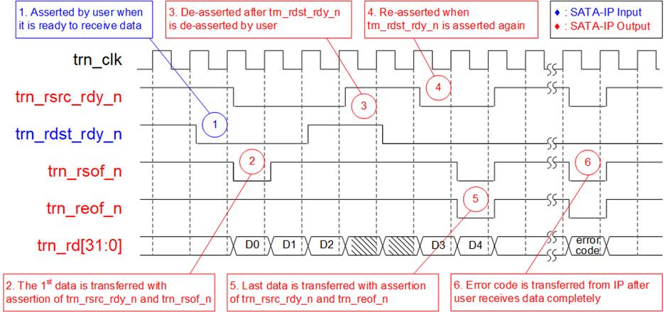
Figure 4: Receive Transaction Interface Timing
As shown in Figure 3 and Figure 4, Error code is used to indicate
that SATA packet is transferred completely or some errors are found. Therefore,
the user should check error code value after finishing transferring each packet.
The detail of error code is shown in Table 3.
Table 3: Error code description.
|
Bit |
Signal Name |
Description |
|
[31:27] |
Reserved |
Always zero |
|
[26] |
Dir |
Current transfer direction flag. 0b: From the Host to SATA IP, 1b: From SATA IP to the Host |
|
[25:24] |
Error |
Error code flag. 00b: No error 01b: Bad/Unknown SATA FIS packet. WTRM primitive is received during read operation or R_ERR primitive is received at the end of write operation. Please check data packet is correct format or not when this error detected. 10b: CRC error. Please check SATA signal quality when this error detected. 11b: Reserved |
|
[23:8] |
Reserved |
Always zero |
|
[7:0] |
FIS Type |
This byte indicates the header of error code packet. EFh is defined to be different from other SATA FIS. |
To cancel current transaction by user, two signals are designed to be SATA IP input - trn_tsrc_dsc_n and trn_rdst_dsc_n. trn_tsrc_dsc_n is applied to cancel current write operation while trn_rdst_dsc_n is applied to cancel current read operation.
After cancelling write operation, trn_tdst_rdy_n status must be monitored to check IP acknowledge, as shown in Figure 5. trn_tdst_rdy_n is de-asserted to 1b after operation is cancelled. The new packet could be transmitted when trn_tdst_rdy_n changes to 0b again.
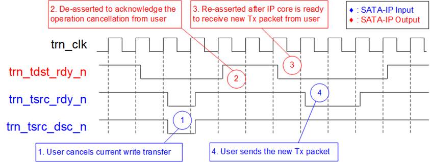
Figure 5: trn_tsrc_dsc_n timing diagram
After cancelling read operation, trn_rsrc_rdy_n is de-asserted to 1b, as shown in Figure 6.
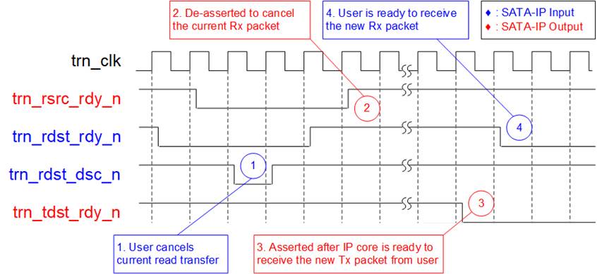
Figure 6: trn_rdst_dsc_n timing diagram
If the target sends SYNC primitives to cancel transmit operation or data collision is detected, trn_tdst_dsc_n will be asserted, as shown in Figure 7. In case of short packet, trn_tdst_dsc_n may be asserted between end of packet and error code.
To re-send the packet after data collision, user needs to wait until trn_tdst_rdy_n is asserted to 0b and the received packet is processed completely.
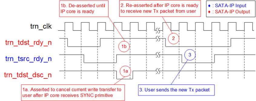
Figure 7: trn_tdst_dsc_n timing diagram
If the target cancels to send the current packet, trn_rsrc_dsc_n will be asserted to 0b. trn_rsrc_rdy_n status changed to 1b to stop current transfer, as shown in Figure 8.
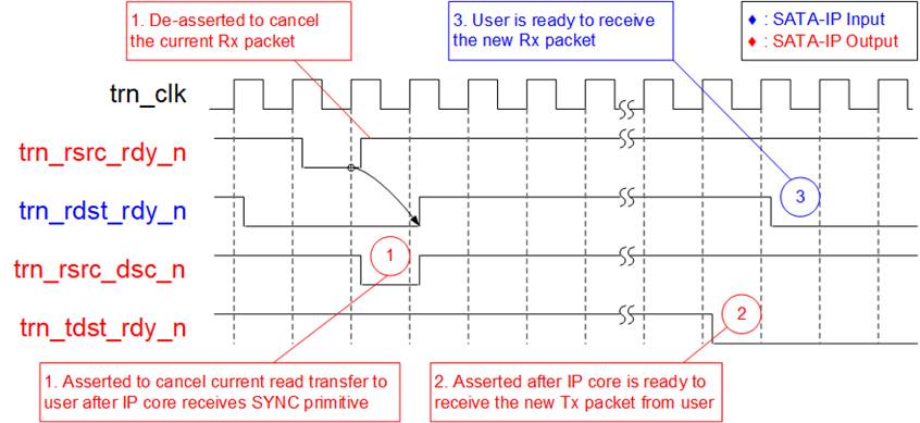
Figure 8: trn_rsrc_dsc_n timing diagram
Verification Methods
The SATA IP functionality was verified by simulation and also proved on real board design by using CycloneV SX SoC board/ArriaV GX Starter kit/StratixV GX board/ArriaV ST SoC board/Arria10 SoC board/Arria10 GX board.
Recommended Design Experience
Experience design engineers with a knowledge of Gigabit Transceiver block and NIOS II EDS should easily integrate this IP into their design. For user board development, compliance with “Altera Transceiver PHY IP Core User Guide” is strongly recommended.
Ordering Information
This product is available directly from Design Gateway Co., Ltd. Please contact Design Gateway Co., Ltd. for pricing and additional information about this product using the contact information on the front page of this datasheet.
Revision History
|
Revision |
Date |
Description |
|
1.6 |
Feb-27-2023 |
Add IPVersion and support Arria10 GX board |
|
1.5 |
Jan-25-2017 |
Update resource utilization |
|
1.4 |
Jun-28-2016 |
Support Arria10 SoC board |
|
1.3 |
Mar-2-2016 |
Support ArriaV ST Soc board |
|
1.2 |
Nov-24-2015 |
Merge V-series to one document |