FPGA setup for TOE/UDP25G-IP with CPU Demo
Rev2.5 6-Jul-23
2 Test environment setup when using FPGA and PC
3 Test environment setup when using two FPGAs
1 Overview
This document provides a guide on setting up an FPGA board and preparing the necessary test environment to run the TOE25G-IP/UDP25G-IP demo or multi-session demo. The user has the option to create two test environments for transferring TCP/UDP payload data via a 25G Ethernet connection using either TOE25G-IP or UDP25G-IP. Figure 1‑1 illustrates these two options.
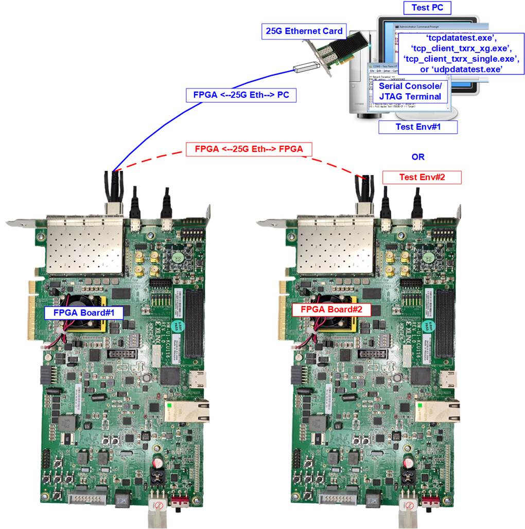
Figure 1‑1 Two test environments for running the demo
The first test environment requires one FPGA board and a PC with a 25G Ethernet card for data transfer. The PC runs a test application, such as �tcpdatatest� (half-duplex test for TOE25G-IP), �tcp_client_txrx_xg� (full-duplex test for TOE25G-IP), �tcp_client_txrx_single� (full-duplex test for multisession TOE25G-IP), or �udpdatatest� (test application for UDP25G-IP). The Serial console or JTAG Terminal is also run on the PC to act as the user interface console.
The second test environment involves two FPGA boards which may be different from each other. Both boards run the TOE25G-IP, multi-session of TOE25G-IP, or UDP25G-IP demo, with different initialization mode assigned (Client, Server, or Fixed-MAC).
The demo is implemented on multiple FPGA boards, each with different settings for RS-FEC features. For specific information of the RS-FEC settings one ach FPGA board, please refer to the table provided below.
Table 1‑1 The features of RS-FEC for TOE25G-IP/UDP25G-IP demo on each board
|
Board name |
RS-FEC feature |
|
TOE25G-IP demo |
|
|
KU15P card |
Disabled |
|
KCU116 |
Enabled |
|
ZCU111 |
Enabled |
|
VCU118 |
Disabled |
|
VCK190 |
Enabled |
|
UDP25G-IP demo |
|
|
KU15P card |
Disabled |
|
KCU116 |
Enabled |
|
ZCU111 |
Enabled |
|
Alveo U250 |
Disabled |
2 Test environment setup when using FPGA and PC
Before running the demo using an FPGA and PC, please prepare the following.
- FPGA development boards: VCK190 (with micro SD for SysCont), VCU118, ZCU111, KCU116, and FB2CGHH@KU15P card
- PC with a 25 Gigabit Ethernet card
- 25G Ethernet cable:
a) VCK190, VCU118, and FB2CGHH@KU15P card: SFP28 transceiver (25GBASE-SR), QSFP28 transceiver (100GBASE-SR), and MTP to 4xLC Fiber cable
b) ZCU111, KCU116: 25G SFP28 Active Optical Cable (AOC).
- USB cable for connecting between FPGA and PC
a) VCK190: a USB type-C cable for programming FPGA and Serial console
b) VCU118 and KCU116 board: two micro USB cables for programming FPGA and Serial console
c) ZCU111: a micro USB cable for programming FPGA and Serial console
d) FB2CGHH@KU15P card: a mini USB cable for programming FPGA and JTAGAURT
- For FB2CGHH@KU15P card, use AB18-PCIeX16 board provided by Design Gateway with ATX power supply to be power board for the card. More details of AB18 card are displayed on following website.
https://dgway.com/ABseries_E.html
- Test application provided by Design Gateway for running on PC
a) TOE25G-IP: �tcpdatatest.exe� and �tcp_client_txrx_xg.exe�
b) Multi-session of TOE25G-IP: �tcpdatatest.exe� and �tcp_client_txrx_single.exe�
c) UDP25G-IP: �udpdatatest.exe�
- Serial console software (except FB2CGHH@KU15P card) such as TeraTerm installed on PC. The console setting is Baudrate=115,200, Data=8-bit, Non-parity, and Stop=1-bit.
Note: FB2CGHH@KU15P card uses JTAG Terminal instead of Serial console.
- Vivado tool for programming FPGA and JTAG Terminal (when using FB2CGHH@KU15P card), installed on PC
Note: The hardware listed below is an example for running the demo.
[1] 25G Network Adapter: Nvidia MCX631102AC-ADAT
[2] 25G Ethernet cable
a) SFP28 to QSFP28 connection (except KCU116)
SFP28 Transceiver: AZS85-S28-M1
https://www.sfpcables.com/25gb-s-sfp28-sr-transceiver-850nm-up-to-100m-2866
QSFP28 Transceiver: AMQ28-SR4-M1
https://www.sfpcables.com/100gb-s-qsfp28-sr4-optical-transceiver-module-1499
MTP to 4xLC Fiber cable: OM4-MTP-8LC-1M
https://www.fs.com/products/68047.html
b) 25G SFP28 Active Optical Cable: S28-AO01 (KCU116)
https://www.fs.com/sg/products/68335.html
[3] Test PC:
Motherboard: Gigabyte Z590 AORUS MASTER (rev. 1.0)
CPU: Intel i7-11700K CPU 3.6 GHz
RAM: 32 GB DDR4
OS: 64-bit Windows10 OS
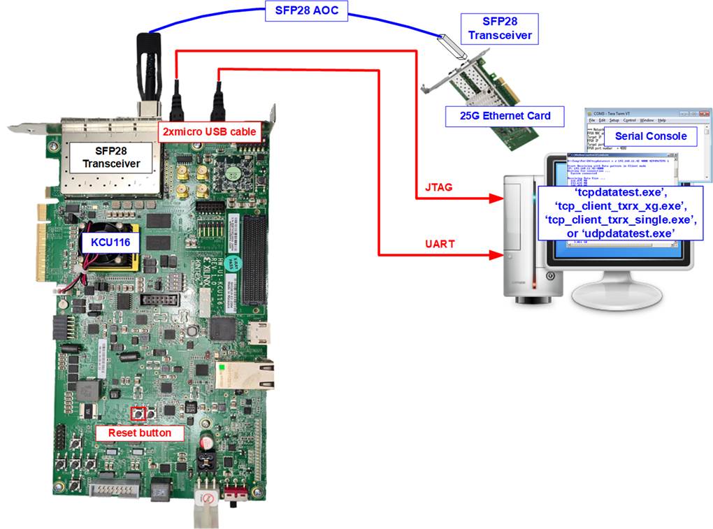
Figure 2‑1 Demo (FPGA <-> PC) on KCU116
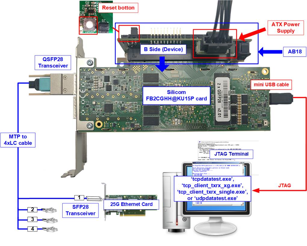
Figure 2‑2 Demo (FPGA <-> PC) on FB2CGHH@KU15P
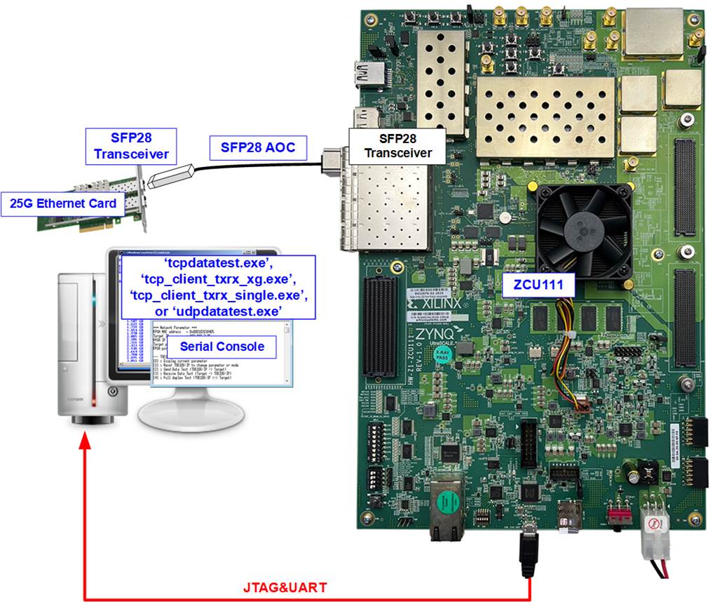
Figure 2‑3 Demo (FPGA <-> PC) on FB2CGHH@KU15P
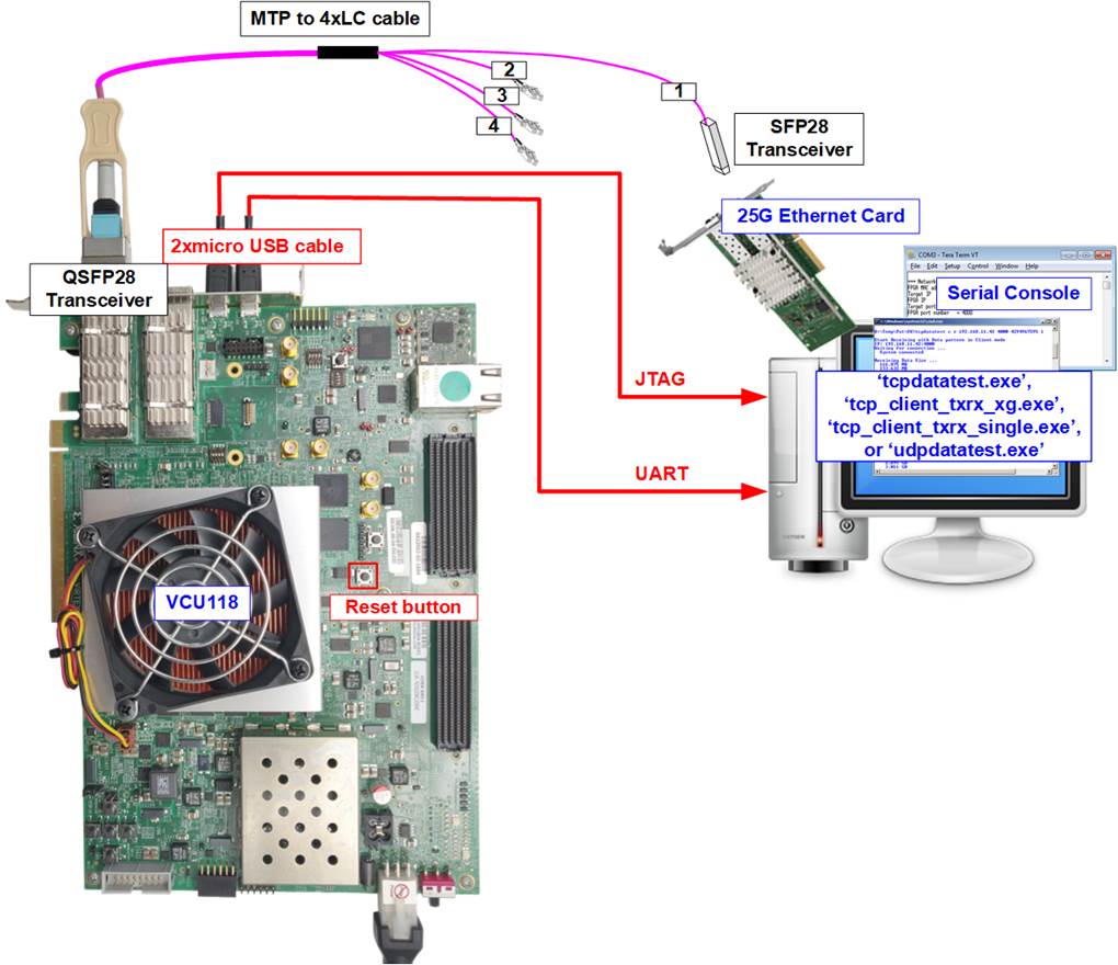
Figure 2‑4 Demo (FPGA <-> PC) on VCU118
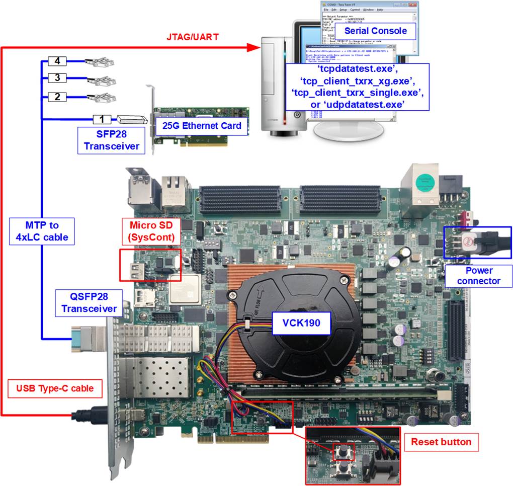
Figure 2‑5 Demo (FPGA <-> PC) on VCK190
The steps for setting up a test environment using an FPGA board and a PC are described below.
1) For ZCU111 board, check the DIPSW setting on the FPGA board. Set SW6=all Ons to use USB-JTAG as shown in Figure 2‑6.
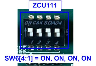
Figure 2‑6 ZCU111 board setting
2) Connect USB cables from the FPGA and PC for JTAG programming and Serial console/JTAGUART.
a) KCU116 and VCU118 board: Connect two micro USB cables
b) VCK190 board: Connect a USB type-C cable
c) FB2CGHH@KU15P card: Connect a mini USB cable
3) Connect the power supply to the FPGA development board/FPGA accelerator card.
a) KCU116 and VCU118 board: Connect Xilinx power adapter 60W (12V)
b) VCK190 board: Connect Xilinx power adapter 180W (12V)
c) FB2CGHH@KU15P card: Connect the card to PC or AB18-PCIeX16 board as below.
i) Confirm that two mini jumpers are inserted at J5 connector on AB18.
ii) Connect ATX power supply to AB board.
iii) Connect PCIe connector on FPGA board to Device Side (B-Side), as shown in Figure 2‑7.

Figure 2‑7 AB18-PCIeX16 connection for power supply of FB2CGHH@KU15P card
4) Connect the FPGA board to the PC via a 25G Ethernet cable.
a) VCK190, VCU118, and FB2CGHH@KU15P: Insert QSFP28 to SFP28 cable by using QSFP(1) connector and plug SFP28 no.1 to 25G Ethernet card on the PC, as shown in Figure 2‑8.
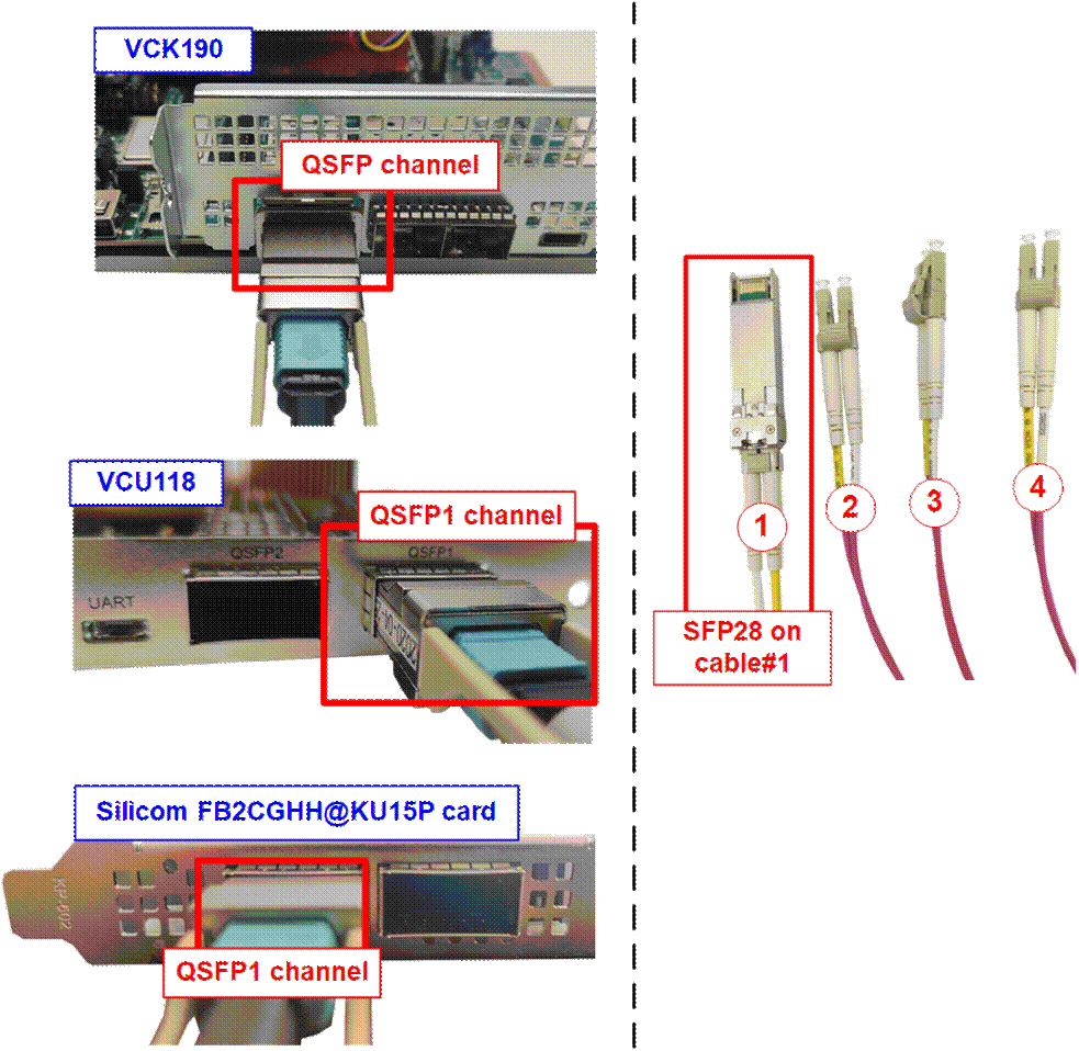
Figure 2‑8 25G connection by using QSFP28 to 4xSFP28 cable
b) KCU116/ZCU111: Insert 25G SFP28 AOC cable between FPGA board (on the left-most channel) and 25G Ethernet card on the PC, as shown in Figure 2‑9.
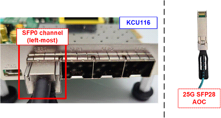
Figure 2‑9 25G connection by 25G SFP28 AOC
5) Connect the other end of the cable by inserting SFP28 transceiver to the 25G Ethernet card on PC.
6) Power on the FPGA board. For VCK190 board, please follow these steps.
i) Insert a micro SD card into the system controller�s SD card socket (J206). Then, set DIP switch (SW11) to be ON OFF OFF OFF to boot from SysCont SD.
Note: For more detailed instructions on setting up the SD card, refer to �Board Setup and Connection� and �Writing the image to micro SD card� topics on the following website.
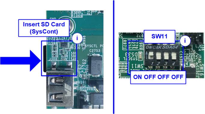
Figure 2‑10 VCK190 board setting
ii) Connect the VCK board to the PC using a USB cable. The PC should detect three USB Serial Ports. Select the third port to check the board boot-up message.
iii) Open a Serial console and connect to the third USB Serial port using the following parameters: Baud rate=115,200, Data=8-bit, Non-parity, and Stop bits=1-bit.
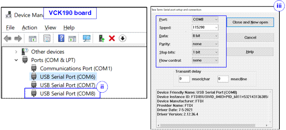
Figure 2‑11 Serial console for boot-up on VCK190
iv) Power on the board and wait until the boot message on the console is completed.
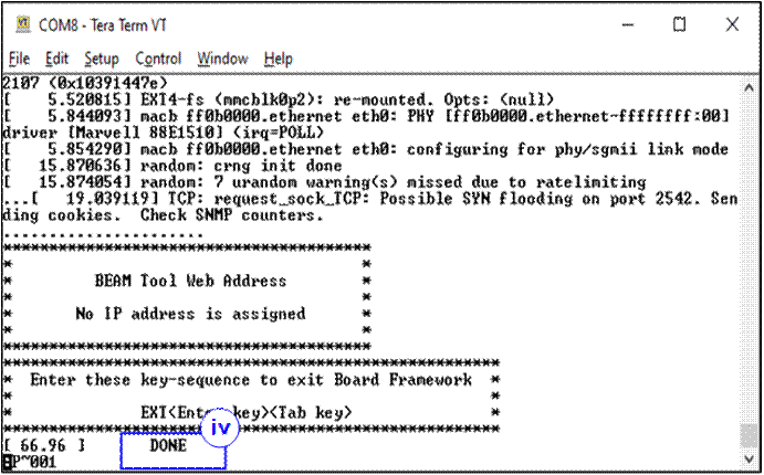
Figure 2‑12 Boot-up message of power-on sequence on VCK190
7) Open Serial console (except FB2CGHH@KU15P card which uses JTAG-Terminal). When connecting FPGA board to PC, multiple COM ports from FPGA connection are detected and displayed on Device Manager.
a) VCU118 and KCU116: Select standard COM port.
b) VCK190 and ZCU111: Select the first USB Serial port.
Use following setting on the Serial console: Baud rate=115,200, Data=8-bit, Non-Parity, and Stop=1.
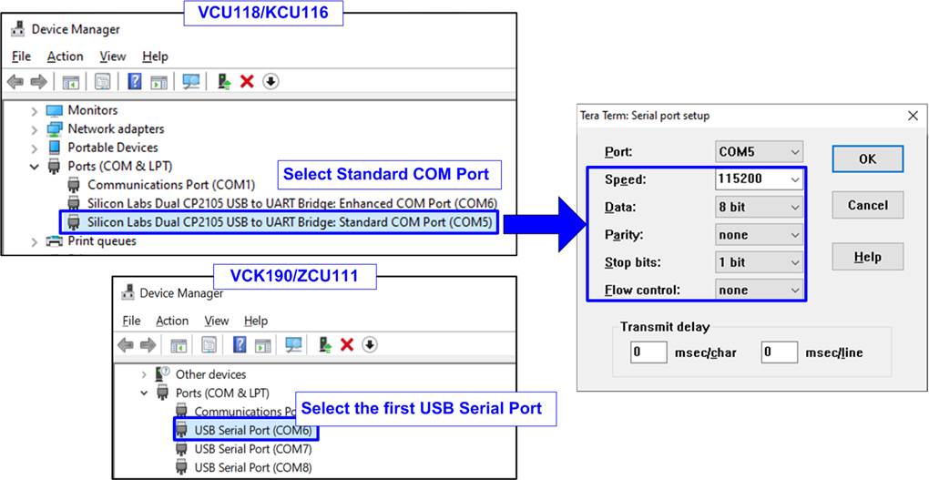
Figure 2‑13 Port for Serial console
8) To configure the programmable clock for the FPGA board, determine whether your board requires a programmable clock setup. If board has already used the desired clock frequency, you do not need to re-configure it.
a) KCU116 board: Use �KCU116 � Board User Interface� application to set the programmable clock to 322.265625 MHz, as shown in Figure 2‑14.
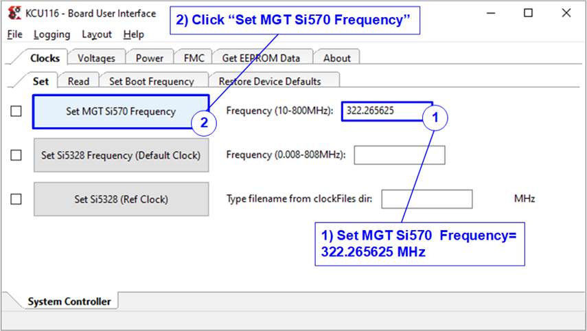
Figure 2‑14 Reference clock programming for KCU116
b) ZCU111 board: Using �ZCU111 � Board User Interface� application as shown in Figure 2‑15
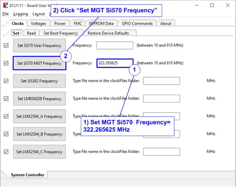
Figure 2‑15 Reference clock programming for ZCU111
c) VCU118 board: Use �VCU118 SCUI� application to set the programmable clock to 322.265625 MHz, as shown in Figure 2‑16.
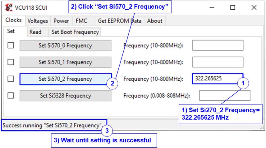
Figure 2‑16 Reference clock programming for VCU118
d) VCK190 board: Use �VCK190 � Board User Interface� application to set the programmable clock to 322.265625 MHz, as shown in Figure 2‑17.
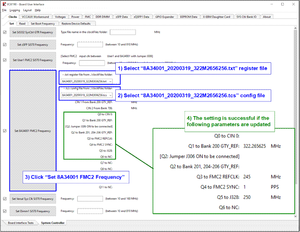
Figure 2‑17 Reference clock programming for VCK190
e) Other boards: No action is required to set up the programmable clock.
9) Download configuration file and firmware to the FPGA board using Vivado tool or Script file, depending on the board.
a) VCU118 and KCU116 boards: Use Vivado tool to program configuration file (bit file), as shown in Figure 2‑18.
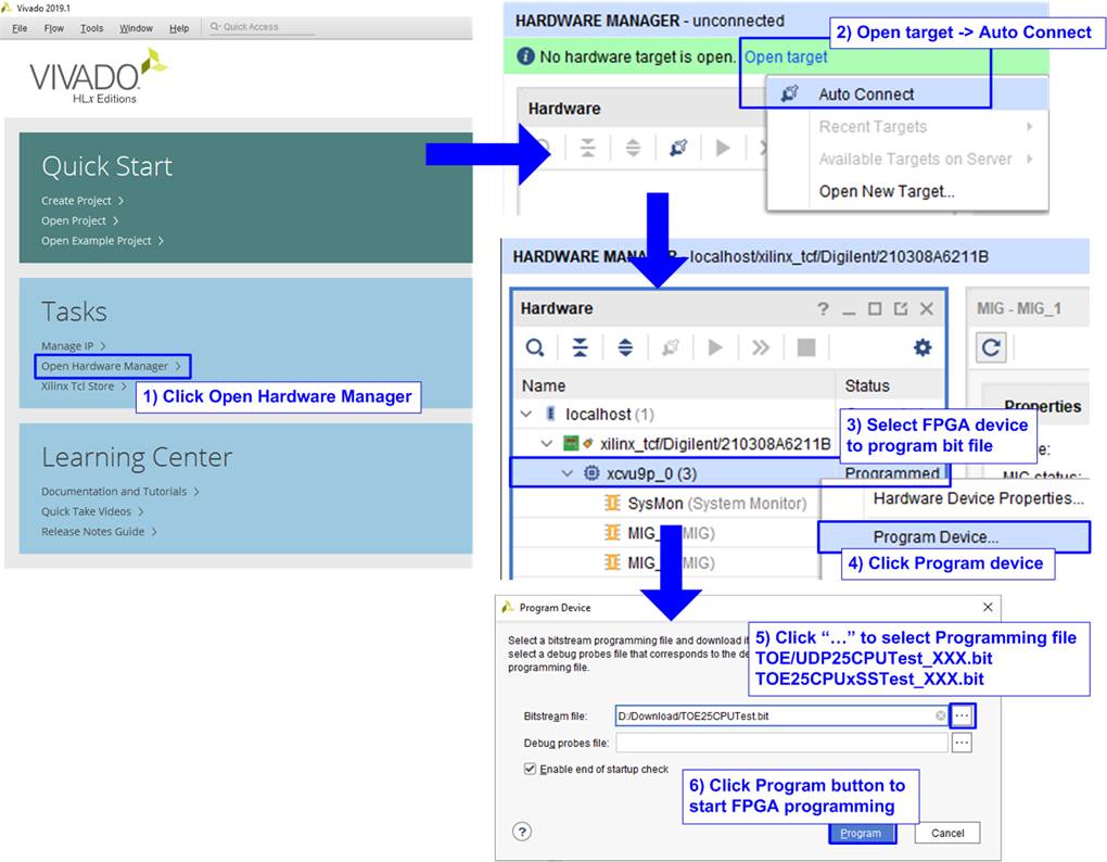
Figure 2‑18 Program bit file by Vivado
b) VCK190 and ZCU111 boards: Use Vivado TCL shell to download the configuration file and the firmware. Browse to the download directory that includes bat file, pdi file, and elf file and type the command to run bat file.
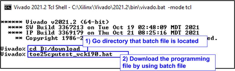
Figure 2‑19 Download demo file on Vivado TCL shell by script file on VCK190
c) FB2CGHH@KU15P card: Use the Vivado TCL shell to download the configuration file and firmware. Browse to the download directory that includes bat file, bit file, and elf file and type the following command.
i) >> TOE25CPUTest_Silicom.bat/UDP25CPUTest_Silicom.bat
Note: This step is to download configuration file and firmware, as shown in Figure 2‑20.
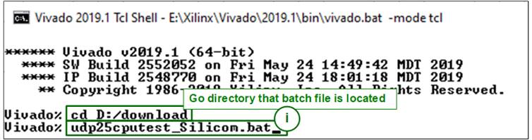
Figure 2‑20 Command script to download demo file on Vivado TCL shel
ii) >> xsdb.bat
iii) >> connect -url tcp:127.0.0.1:3121
iv) >> targets -set -filter {name =~"*Debug*"}
v) >> jtagterminal -start
vi) >> con
Note Upon all above steps are completed, JTAGUART module is connected and JTAG terminal is executed to be the user console, as shown in Figure 2‑21.
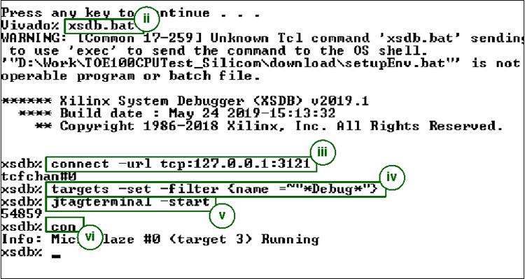
Figure 2‑21 Open JTAG Terminal
10) Upon opening the Serial console/JTAG Terminal, welcome message will be displayed.
i) Input �0� to initiate the TOE25G-IP/UDP25G-IP in Client mode that asks for the PC MAC address through sending ARP request packet.
ii) The default parameter in Client mode will be shown on the console.
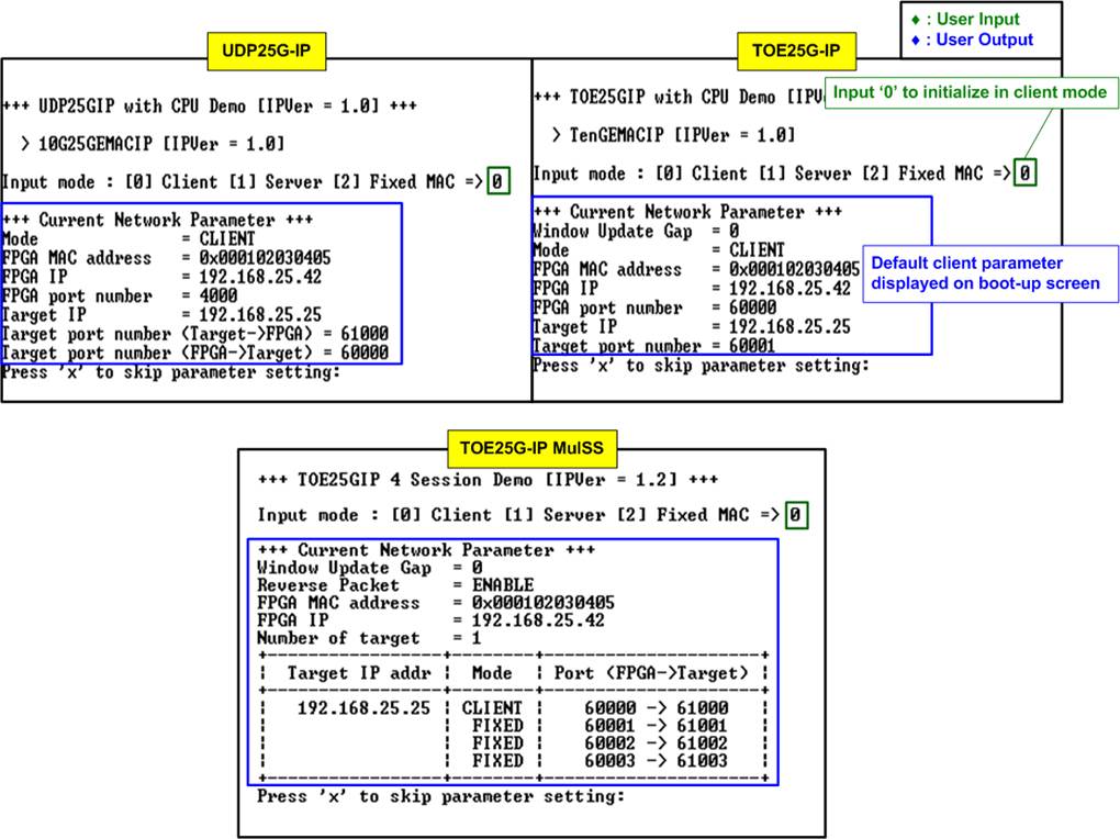
Figure 2‑22 Message after system boot-up
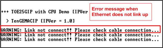
Figure 2‑23 Error message when ethernet connection link down
iii) If the user wishes to skip parameter setting and use default parameters to start the system initialization, input �x� as shown in Figure 2‑24. If any other keys are entered, the menu for changing parameter will appear, similar to the �Reset TCPIP/UDPIP parameters� menu. The examples of running the main menu of TOE25G-IP, Multisession of TOE25G-IP, and UDP25G-IP are described in
�dg_toe25gip_cpu_instruction�, �dg_toe25gip_4ss_instruction�, and
�dg_udp25gip_instruction� documents, respectively.
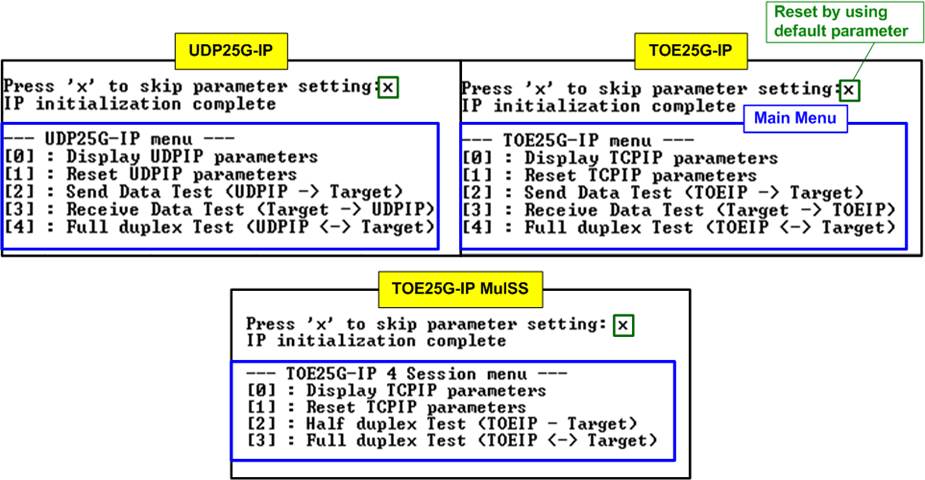
Figure 2‑24 Initialization complete
Note: Transfer performance in the demo is limited by the PC performance. The best performance can be achieved when the test is run using FPGA-to-FPGA connection.
3 Test environment setup when using two FPGAs
Before running the test, please prepare following test environment.
- Two FPGA development boards, which can be either the same or different boards: VCK190 (with micro SD for SysCont), VCU118, ZCU111, KCU116, and FB2CGHH@KU15P card
- 25G Ethernet cable:
a) VCK190, VCU118 and FB2CGHH@KU15P card: SFP28 transceiver (25GBASE-SR), QSFP28 transceiver (100GBASE-SR), and MTP to 4xLC Fiber cable
b) ZCU111 and KCU116: 25G SFP28 Active Optical Cable (AOC)
- USB cable for connecting from the FPGA to the PC
a) VCK190: a USB type-C cable for programing the FPGA and Serial console
b) KCU116 and VCU118: two micro USB cables for programming the FPGA and Serial console
c) ZCU111: a micro USB cable for programming the FPGA and Serial console
d) FB2CGHH@KU15P card: a mini USB cable for programming the FPGA and JTAGUART
- Serial console software (except FB2CGHH@KU15P card) such as TeraTerm, installed on PC. The console setting is Baudrate=115,200, Data=8-bit, Non-parity, and Stop=1-bit.
Note: FB2CGHH@KU15P card uses JTAG Terminal instead of Serial console.
- Vivado tool for programming the FPGA and JTAG Terminal (when using FB2CGHH@KU15P card), installed on PC
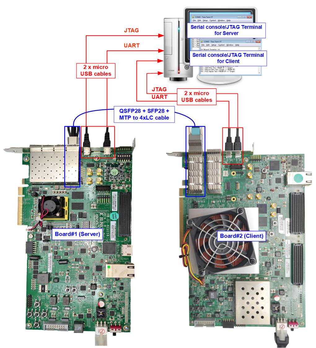
Figure 3‑1 TOE25G-IP/UDP25G-IP with CPU demo (FPGA<->FPGA)
The steps for setting up a test environment using two FPGAs are described below.
To get started with the demo, follow steps 1) � 8) of topic 2 (Test environment setup when using FPGA and PC) to set up the FPGA board and SFP28/QSFP28 connection. Once you have completed the configuration for two FPGA boards, a menu will be displayed on the Serial console/JTAG Terminal for selecting Client mode, Server mode, or Fixed MAC mode. Follow the detailed steps below to continue the demo.
1) Open the Serial console/JTAG Terminal for FPGA board#1 and FPGA board#2, which are set to initialize in Server/Client/Fixed-MAC mode. An example to initialize by Server-Client mode is below.
i) Set �1� on the console of FPGA board#1 for running in Server mode.
ii) Set �0� on the console of FPGA board#2 for running in Client mode.
iii) The default parameters for the selected mode will be displayed on the console, as shown in Figure 3‑2.
Note: The rules for setting the initialization mode are below.
· If the first board is initialized in Server mode, the other board must be initialized in Client mode.
· If the first board is initialized in Fixed MAC mode, the other board can be run in Client mode or Fixed MAC mode.
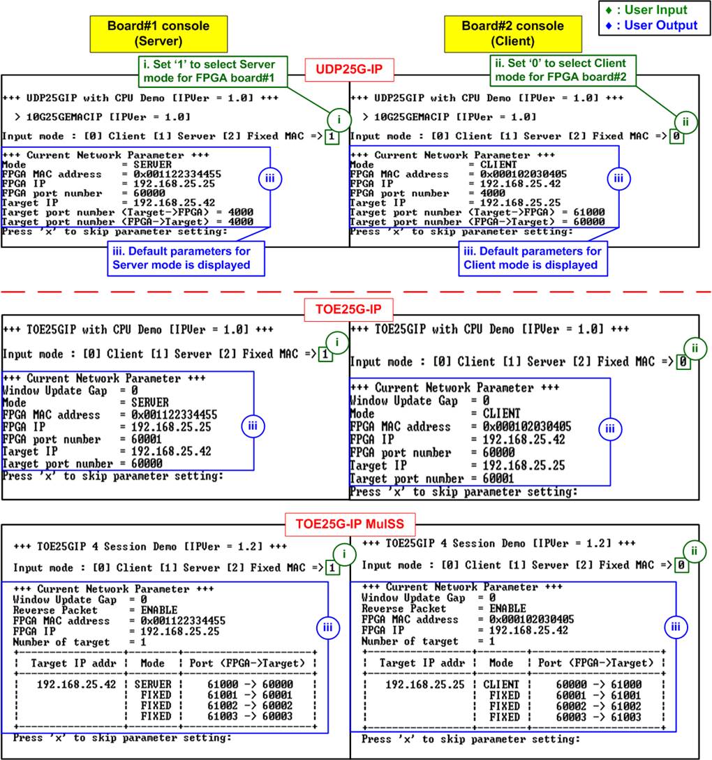
Figure 3‑2 Input mode
2) Input �x� to use default parameters or use other keys to change parameters. The parameters of Server mode must be set before Client mode. The details are divided into two parts, running the TOE25G-IP demo and running the UDP25G-IP demo.
When running single-session or multi-session of TOE25G-IP,
i) Set parameters on the Server console (board#1 console).
ii) Set parameters on the Client console (board#2 console) to start IP initialization by transferring ARP packet.
iii) After finishing the initialization process, �IP initialization complete� and the main menu are displayed on the Server and Client consoles.
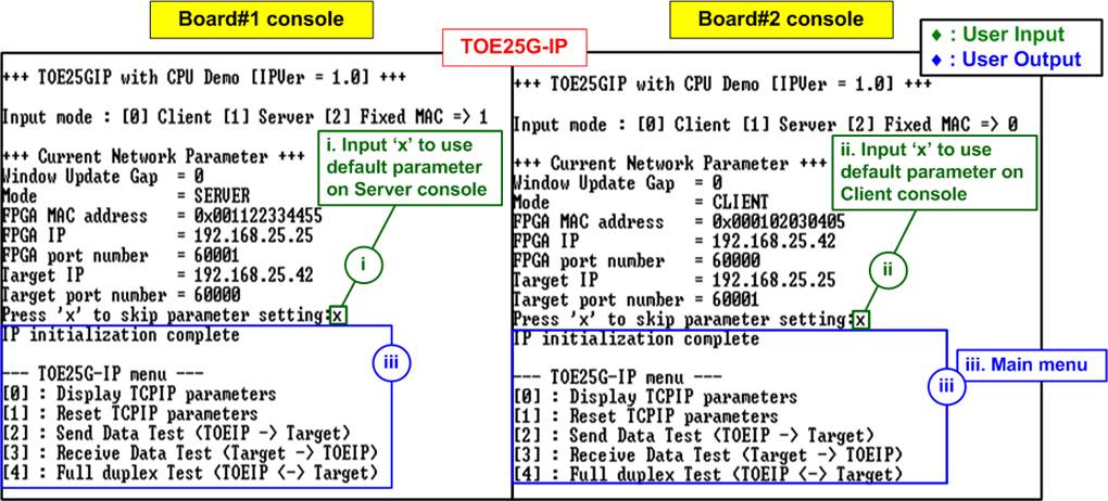
Figure 3‑3 Main menu of TOE25G-IP (Single-session)
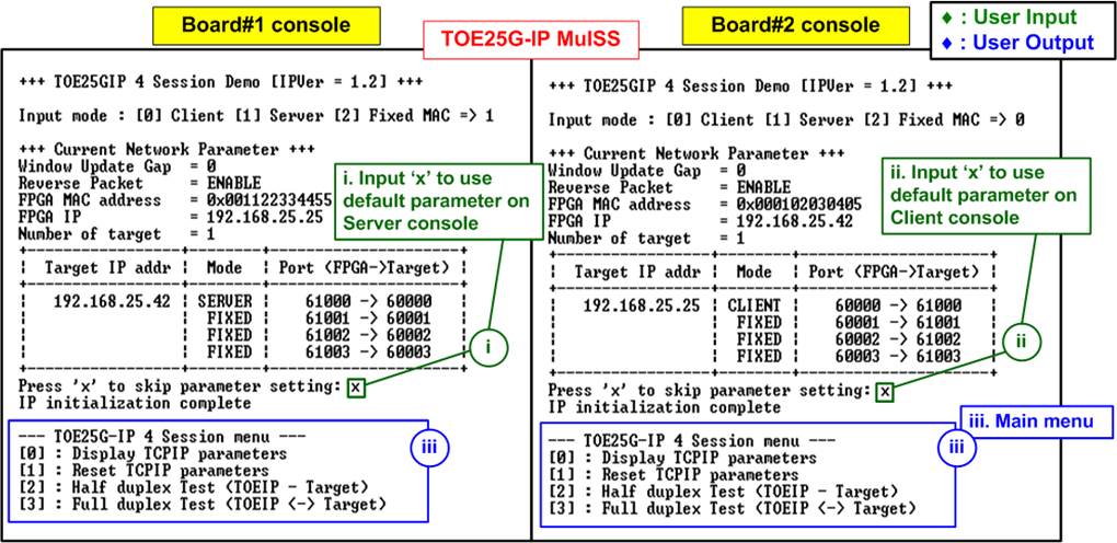
Figure 3‑4 Main menu of TOE25G-IP (Multi-session)
When running UDP25G-IP,
i) For Server mode (board#1 console), if user does not change the default parameters, input �x� to skip parameter setting.
ii) For Client mode, the user must change Target port number (Target->FPGA) to use same value as Target port number (FPGA->Target).
iii) After finishing initialization process, �IP initialization complete� and the main menu will be displayed on the Server and Client consoles.
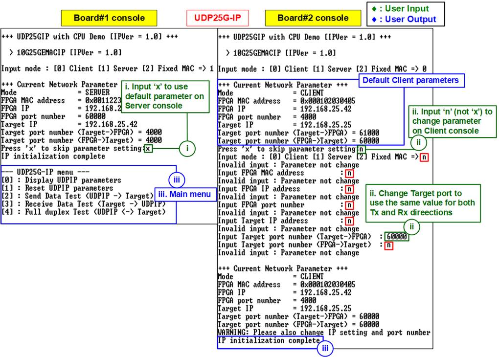
Figure 3‑5 Main menu of UDP25G-IP
4 Revision History
|
Revision |
Date |
Description |
|
2.5 |
25-May-23 |
1) Update full-duplex test application from �tcp_client_txrx_40G� to �tcp_client_txrx_xg�. 2) Add RS-FEC feature lists on each demo |
|
2.4 |
13-Mar-23 |
Add Figure 2‑6 for setting ZCU111 board |
|
2.3 |
9-Mar-23 |
Add ZCU111 board |
|
2.2 |
13-Jan-23 |
Add multi-session demo |
|
2.1 |
12-Jul-22 |
Add VCK190 |
|
2.0 |
7-Jun-21 |
Add UDP25G-IP |
|
1.1 |
15-Sep-20 |
Add KCU116 |
|
1.0 |
5-Aug-20 |
Initial version release |