NVMe IP Core for PCIe switch Data Sheet
Control interface of dgIF typeS

Core Facts |
|
|
Provided with Core |
|
|
Documentation |
Reference Design Manual Demo Instruction Manual |
|
Design File Formats |
Encrypted hdl File |
|
Instantiation Templates |
VHDL |
|
Reference Designs & Application Notes |
QuartusII Project, See Reference Design Manual |
|
Additional Items |
Demo on Arria10 GX development kit |
|
Support |
|
|
Support Provided by Design Gateway Co., Ltd. |
|
Design Gateway Co.,Ltd
E-mail: ip-sales@design-gateway.com
URL: www.design-gateway.com
Features
· NVMe host controller for access one NVMe SSD by direct connection or up to four NVMe SSDs by connection through one PCIe switch
· No need for CPU and external memory
· Include 256 Kbyte RAM to be data buffer
· Simple user interface by dgIF typeS to access one device at a time
· Support six commands, i.e. Identify, Shutdown, Write, Read, SMART, and Flush
· Supported NVMe device
· Base Class Code:01h (mass storage), Sub Class Code:08h (Non-volatile), Programming Interface:02h (NVMHCI)
· MPSMIN (Memory Page Size Minimum): 0 (4Kbyte)
· MDTS (Maximum Data Transfer Size): At least 5 (128 Kbyte) or 0 (no limitation)
· LBA unit: 512 bytes or 4096 bytes
· User clock frequency must be more than or equal to PCIe clock (250 MHz for PCIe Gen3)
· Operating with Avalon-ST Hard IP for PCI Express from Intel by using 128-bit Avalon-ST bus interface
· Available reference design
· Arria10 GX development board with AB18-PCIeX16/AB16-PCIeXOVR adaptor board
· Customized service for following features
· Additional NVMe commands
· RAM size or RAM type (URAM) modification
· Support more than four NVMe SSDs
Table 1: Example Implementation Statistics
|
Family |
Example Device |
Fmax (MHz) |
Logic utilization (ALMs) |
Registers |
Pin |
Block Memory bit1 |
Design Tools |
|
Arria10 GX |
10AX115S2F45I1SG |
300 |
2102 |
4381 |
- |
2,162,688 |
QuartusII 16.0 |
Applications
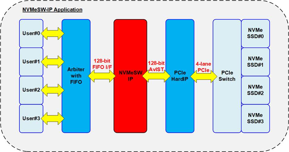
Figure 1: NVMeSW IP Application
NVMeSW IP Core integrated with Avalon-ST PCIe Hard IP from Intel (PCIe hard IP) is ideal to access NVMe SSD without CPU and external memory such as DDR. NVMeSW IP can access more than one SSD through PCIe switch, as shown in Figure 1. By designing Arbiter including the FIFO for bufferring the data, multiple user logics can be accessed the different NVMe SSDs through one set of NVMeSW IP, PCIe hard IP and PCIe switch. As a result, each SSD can store the different data stream from the different data source at very high performance. For more specific applications, we also provides alternative IP as follows.
Random Access NVMe IP Core– To access NVMe SSD with multiple commands, individual address for each. Recommended for the application which requires the access in non-contiguous area, stream data recording without specified length or application that one SSD can be accessed by multiple users.
https://dgway.com/raNVMe-IP_A_E.html
NVMe IP Core with PCIe Gen 3 Soft IP – When the selected FPGA does not have enough PCIe hard IP for the application.
https://dgway.com/NVMeG4-IP_A_E.html
General Description
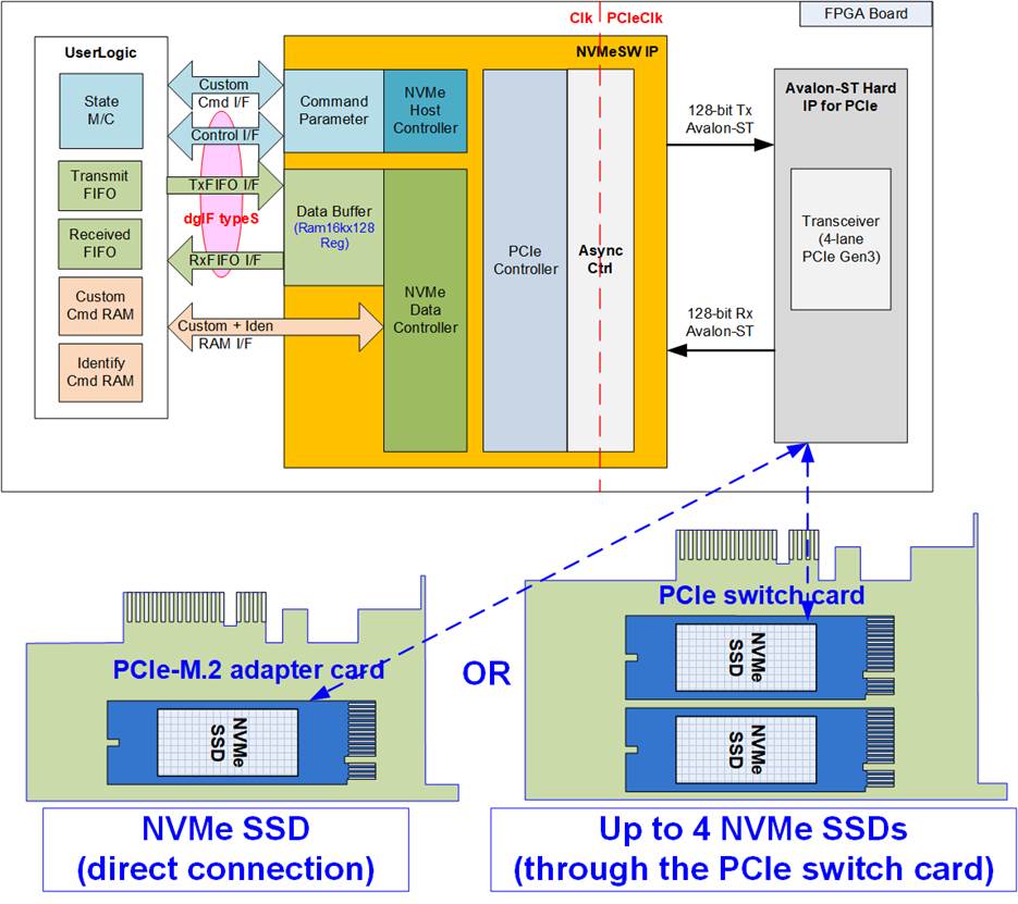
Figure 2: NVMeSW IP Block Diagram
NVMeSW IP implements as host controller to access NVMe SSD following NVM express standard. Physical interface of NVMe SSD is PCIe. The lower layer hardware is implemented by using Avalon-ST PCIe Hard IP from Intel.
NVMeSW IP supports six NVMe commands, i.e. Identify, Shutdown, Write, Read, SMART and Flush command by using two user interface groups. First is Control interface for transferring command and the parameters. Another is Data interface for transferring data when the command must have the data transferring. The Control interface and Data interface for Write/Read command use dgIF typeS format. Control interface of dgIF typeS has start address and transfer length with asserting the request signal while Data interface of dgIF typeS is the FIFO interface.
Although up to four NVMe SSDs could be connected to NVMeSW IP, only one SSD is operated at a time. NVMeSW IP has the signal for selecting active device, called UserDevSel. The device selection is the input parameter for all commands.
Note: When connecting through PCIe switch, the FPGA supports only one-level PCIe switch. More than one PCIe switch card connected as multiple-level are not supported. All SSDs are connected to the same PCIe switch.
SMART and Flush command require the specific interface, called Custom command interface, which consists of Ctm I/F for control path and Ctm RAM I/F for data path. Furthermore, Identify command has its own data interface, named Iden RAM I/F, as shown in Figure 2.
During initialization or running some commands, error signal may be asserted by NVMeSW IP if some abnormal conditions are found. The IP includes the error status to check the more details of error condition. To recover error status, NVMeSW IP and all SSDs must be reset.
There is one limitation about clock frequency of user logic. Transmit packet to PCIe hard IP must be sent continuously until end of packet. Therefore, data must be valid every clock between start of packet and end of packet. To support this feature, user logic clock frequency must be more than or equal to PCIe clock frequency (250 MHz for PCIe Gen3) to have the bandwidth of transmit logic higher than or equal to PCIe hard IP bandwidth.
The reference design on FPGA evaluation boards are available to evaluate before purchasing.
Functional Description
Figure 3 shows operation sequence of NVMe IP after IP reset is released.
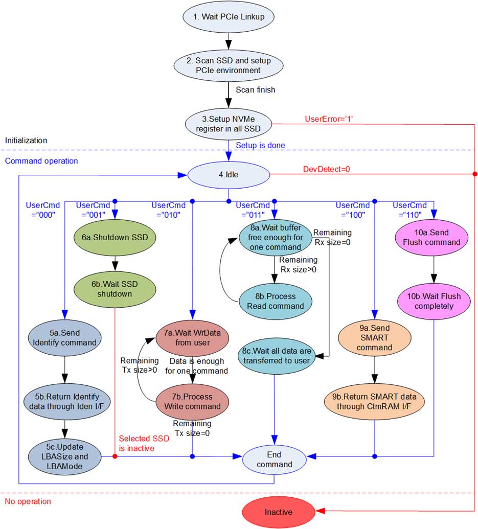
Figure 3: NVMeSW IP Operation Flow
The operation of NVMeSW IP is described as follows.
1) IP waits until PCIe is ready by monitoring Linkup status from PCIe IP core.
2) IP reads PCIe configuration to scan device connection type (direct connection or connection through PCIe switch) and scan the number of SSDs in the connection. After that, the IP sets up PCIe environment of all SSDs (up to 4 SSDs).
3) IP sets up NVMe parameters to one SSD at a time. When multiple SSDs are connected, the setup process is run many times to setup all SSDs. After finishing the setup process, IP enters to the Idle state to wait for a new command request from the user. If some SSDs are detected during setup process, the IP changes to the Inactive state.
4) In the Idle state, IP is ready to receive command from user. To start the new command operation, user sets UserCmd with the input parameters and sets UserDevSel to select the active SSD.
5) The 1st command from user must be Identify command (UserCmd=”000”) to update LBASize (disk capacity) and LBAMode (LBA unit=512 bytes or 4 Kbytes). When many SSDs are connected through PCIe switch, Identify command must be sent many times to get the information of all SSDs.
6) The last command before power down the system must be Shutdown command (UserCmd=”001”). This command is recommended to guarantee SSD powered down in a good sequence. Without Shutdown command, Write data in SSD cannot be guaranteed. After finishing Shutdown command, the selected SSD changes to inactive state. Next, NVMeSW IP changes to the Idle state to receive new command for the ramaining active SSDs. The inactive SSD could not be accessed until the system is reset.
Note: After all SSDs are inactive by Shutdown command, the state changes from the Idle state to the Inactive state. NVMeSW IP does not receive any command in Inactive state until resetting the IP.
7) For Write command (UserCmd=”010”), the maximum data size of one command is 128 Kbytes. If total length from user is more than 128 Kbytes, repeat step 7a) – 7b) for many times.
a) The IP waits until Write data, sent by user, is enough for one command (transfer size of one command in NVMeSW IP is 128 Kbytes, except the last loop which could be less than 128 Kbytes).
b) The IP sends Write command to SSD and then waits until the status is returned from SSD. The IP changes to the Idle state when total data is completely transferred. Otherwise, the IP goes back to step 7a) to send the next Write command.
8) Similar to Write command, Read command (UserCmd=”011”) must be sent to the SSD many times when total length from user is more than 128 Kbytes. As a result, step 8a) – 8b) are repeated many times.
a) The IP waits until the free space of data buffer in NVMeSW IP is enough for one command. If remaining transfer size is equal to zero, the IP skips to step c).
b) The IP sends Read command to SSD. After that, goes back to step a) to check the remaining transfer size and the free space of data buffer.
c) IP waits until all data are completely transferred from data buffer to user logic and then changes to the Idle state. Therefore, data buffer is empty after finishing Read command.
9) For SMART command (UserCmd=”100”), 512-byte data is returned after finishing the operation.
a) IP sends Get Log Page command to read SMART/Health information from SSD.
b) 512-byte data is returned from the SSD. The IP forwards the data through Custom command RAM interface (CtmRamAddr=0x000 – 0x01F).
10) For Flush command (UserCmd=”110”), there is no data transferring during the operation.
a) IP sends Flush command to the SSD.
b) IP waits until SSD returns status to complete the operation.
To design NVMe host controller, NVMeSW IP implements two protocols, i.e. NVMe protocol for interfacing with user and PCIe protocol for interfacing with PCIe hard IP. The details of the hardware inside NVMeSW IP are described as follows.
NVMe
NVMeSW IP supports six commands, i.e. Identify, Write, Read, SMART, Flush and Shutdown command which can be divided to two command types, i.e. Admin command and NVM command. NVMeSW IP supports three Admin commands, i.e. Identify, Shutdown and SMART command and three NVM commands, i.e. Write, Read and Flush command. After finishing the command, the status returned from the SSD is latched to AdmCompStatus signal when running Admin command or IOCompStatus signal when running NVM command.
The parameters of Write or Read command are set by Control interface of dgIF typeS while the parameters of SMART or Flush command are set by CtmSubm of Ctm interface. Data interface for Write or Read command is transferred by FIFO interface, a part of dgIF typeS, which is finally connected with 256-Kbyte buffer inside the IP. The data interface of other commands has its own interface, i.e. Identify RAM for Identify command and Custom RAM for SMART command.
The details of each submodule are described as follows.
· NVMe Host Controller
NVMe host controller is the main controller in NVMeSW IP. The operation is split into two phases. First is the initialization phase which is once run after the system is boot up for setting NVMe register inside the SSD. After finishing the initialization phase, the next phase is the command operation phase. The order of transmitted and received packet is controlled by NVMe host controller.
To operate the command, the parameters of each command are prepared in Command Parameter and then forwarded to AsyncCtrl. After finishing the command, the status packet returned from SSD is monitored by NVMe host controller to check if no error is found. When the command needs to transfer data such as Write, Read, SMART and Identify command, NVMe host controller must also handle with NVMe data controller.
· Command Parameter
This module is designed to prepare command packet for SSD and decode status packet returned from SSD.
Typically, the command consists of 16 Dwords (1 Dword = 32-bit). When running Identify, Shutdown, Write or Read command, all 16 Dwords are created by Command parameter, following the user inputs on dgIF typeS. When running SMART and Flush command, all 16 Dwords are directly loaded via CtmSubmDW0-CtmSubmDW15 of Ctm interface.
· Data Buffer (Ram16kx128Reg)
Data buffer is created by IP catalog inside Quartus tools for storing data which is transferred in Write or Read command. It is implemented as two-port RAMs with simple dual port memory mode (one read port and one write port). RAM size is 16kx128-bit with byte enable for Write port. Read output port includes register, so read data latency is equal to two clock cycles. The memory block type is set as Auto to allow the tool using embedded memory block.
· NVMe Data Controller
This module is operated when the command must transfer the data, i.e. Identify, SMART, Write and Read command. There are three data interfaces for transferring with the SSD, i.e. FIFO interface with 256-Kbyte buffer when running Write or Read command, Custom command RAM interface when running SMART command or Identify RAM interface when running Identify command.
When running Write or Read command, the address of the data buffer is controlled by NVMe data controller.
PCIe
The PCIe standard is the outstanding lower layer protocol for very high speed application. The NVMe standard is the protocol which is run over PCIe protocol. In the initialization process, NVMe layer is setup after finishing PCIe layer setup. Two modules are designed to support PCIe protocol, i.e. PCIe controller and AsyncCtrl. More details of each module are described as follows.
· PCIe Controller
During initialization process, PCIe controller sets up PCIe environment of all SSDs via Avalon-ST interface. the same interface is applied to transfer the command and data packet with NVMe module which are converted to be PCIe packet by PCIe controller. On the other hand, the received PCIe packet is decoded and converted to be NVMe packet for NVMe module by this module.
NVMeSW IP must scan the connected device and detect the device type. If no NVMe SSD is detected in the chain, the error flag is asserted.
· AsyncCtrl
AsyncCtrl includes asynchronous registers and buffers to support signal and data clock-crossing. Most logics in NVMeSW IP run on user clock domain while PCIe hard IP runs on PCIe clock domain. Avalon-stream interface of PCIe hard IP must transfer data of each packet continuously, so the user bandwidth must be greater than or equal to PCIe bandwidth by running at higher or the same clock frequency of PCIe clock.
User Logic
Avalon-ST PCIe Hard IP
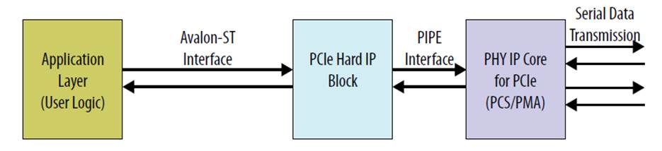
Figure 4: Architecture of Avalon-ST PCIe Hard IP
PCIe Hard IP Block embeds the PCIe protocol stack into the Intel FPGA. The hard IP block includes the transceiver modules, physical layer, data link layer and transaction layer. NVMeSW IP uses one PCIe hard IP which can connect to one PCIe switch with up to four NVMe SSDs. More connections can be customized. By using multiple IPs, more SSDs can be connected to the system. More details of PCIe hard IP are described in following document.
Intel Arria10 and Intel Cyclone 10 GX Avalon-ST Interface for PCIe Solutions User Guide
https://www.intel.com/content/dam/www/programmable/us/en/pdfs/literature/ug/ug_a10_pcie_avst.pdf
Core I/O Signals
Descriptions of all signal I/Os are provided in Table 2 and Table 3.
Table 2: User logic I/O Signals (Synchronous to Clk signal)
|
Signal |
Dir |
Description |
|
Control I/F of dgIF typeS |
||
|
RstB |
In |
Synchronous reset signal. Active low. De-assert to ‘1’ when Clk signal is stable. |
|
Clk |
In |
System clock for running NVMeSW IP. The frequency must be more than or equal to PCIeClk which is output from PCIe hard IP (250 MHz for PCIe Gen3). |
|
DevDetect[3:0] |
Out |
Detected SSD status. Each bit shows one SSD status. Bit[0], [1], [2] and [3] are SSD#0, #1, #2 and #3 respectively. ‘0’: Not found, ‘1’: NVMe SSD detected. DevDetect signal is valid after the IP completes initialization process (UserBusy=’0’). When one SSD is connected to the FPGA directly, DevDetect is equal to “0001”. Four bits are all asserted to ‘1’ when four SSDs are connected. After user sends Shutdown command, DevDetect of the selected SSD is de-asserted to ‘0’. |
|
UserDevSel[1:0] |
In |
Selects the active SSD for running the command. Set “00”, “01”, “10” or ”11” for selecting SSD#0, #1, #2 or #3 respectively. Before selecting the device, please check DevDetect signal that the selected SSD is still active. |
|
UserCmd[2:0] |
In |
User Command. Valid when UserReq=’1’. (“000”: Identify, “001”: Shutdown, “010”: Write SSD, “011”: Read SSD, “100”: SMART, “110”: Flush, “101”/”111”: Reserved) |
|
UserAddr[47:0] |
In |
Start address to write/read SSD in 512-byte unit. Valid when UserReq=’1’. In case LBA unit = 4 Kbyte, UserAddr[2:0] must be always set to “000” to align 4-Kbyte unit. In case LBA unit = 512 byte, it is recommended to set UserAddr[2:0]=”000” to align 4-Kbyte size (SSD page size). Write/Read performance of most SSDs is reduced when start address is not aligned to page size. |
|
UserLen[47:0] |
In |
Total transfer size to write/read SSD in 512-byte unit. Valid from 1 to (LBASize-UserAddr). In case LBA unit = 4 Kbyte, UserLen[2:0] must be always set to “000” to align 4-Kbyte unit. Valid when UserReq=’1’. |
|
UserReq |
In |
Asserts to ‘1’ to send the new command request and de-asserts to ‘0’ after IP starts the operation by asserting UserBusy to ‘1’. This signal can be asserted when the IP is Idle (UserBusy=’0’). Command parameters (UserDevSel, UserCmd, UserAddr, UserLen and CtmSubmDW0-DW15) must be valid and stable during UserReq=’1’. UserDevSel, UserAddr and UserLen are inputs for Write/Read command while UserDevSel and CtmSubmDW0-DW15 are inputs for SMART/Flush command. |
|
UserBusy |
Out |
Asserted to ‘1’ when IP is busy. New request must not be sent (UserReq to ‘1’) when IP is busy. |
|
LBASize0[47:0] - LBASize3[47:0] |
Out |
Total capacity of SSD#0-#3 in 512-byte unit. Default value is 0. LBASize0, 1, 2 and 3 are the size of SSD#0, #1, #2 and #3 respectively. LBASize of each SSD is valid after finishing Identify command. |
|
LBAMode[3:0] |
Out |
LBA unit size of SSD (‘0’: 512 bytes, ‘1’: 4 Kbytes). Default value is 0. Bit[0], [1], [2] and [3] are referred to SSD#0, #1, #2 and #3 respectively.- This value is valid after finishing Identify command. |
|
UserError |
Out |
Error flag. Assert when UserErrorType is not equal to 0. The flag can be cleared by asserting RstB to ‘0’. |
|
UserErrorDev[1:0] |
Out |
Show the active device which is in operating. So, UserErrorDev can be applied to check the error device number. |
|
Signal |
Dir |
Description |
|
Control I/F of dgIF typeS |
||
|
UserErrorType[31:0] |
Out |
Error status. [0] – Error when no SSD is detected during initialization process. Note: This flag is not asserted after all SSDs finish Shutdown command. [1] – Error from CAP (Controller capabilities) register which may be caused from - MPSMIN (Memory Page Size Minimum) is not equal to 0. - NVM command set flag (bit 37 of CAP register) is not set to 1. - DSTRD (Doorbell Stride) is not 0. - MQES (Maximum Queue Entries Supported) is more than or equal to 7. More details of each register can be checked from NVMeCAPReg signal. [2] – Error when Admin completion entry is not returned until timeout. [3] – Error when status register in Admin completion entry is not 0 or phase tag/command ID is invalid. Please see more details from AdmCompStatus signal. [4] – Error when IO completion entry is not returned until timeout. [5] – Error when status register in IO completion entry is not 0 or phase tag is invalid. Please see more details from IOCompStatus signal. [6] – Error when Completion TLP packet size is not correct. [7] – Error when PCIe hard IP detects Error correction code (ECC) error from the internal buffer. [8] – Error from Unsupported Request (UR) flag in Completion TLP packet. [9] – Error from Completer Abort (CA) flag in Completion TLP packet. [15:10] – Reserved [16] - Error from unsupport LBA unit (LBA unit is not equal to 512 bytes or 4 Kbytes) [31:17] – Reserved Note: Timeout period of bit[2]/[4] is set from TimeOutSet input. |
|
Data I/F of dgIF typeS |
||
|
UserFifoWrCnt[15:0] |
In |
Write data counter of Receive FIFO. Used to check full status. If total FIFO size is less than 16 bits, please fill ‘1’ to upper bit. |
|
UserFifoWrEn |
Out |
Asserted to ‘1’ to write data to Receive FIFO during running Read command. |
|
UserFifoWrData[127:0] |
Out |
Write data bus of Receive FIFO. Valid when UserFifoWrEn=’1’. |
|
UserFifoRdCnt[15:0] |
In |
Read data counter of Transmit FIFO. Used to check data size stored in FIFO. If FIFO size signal is less than 16 bits, please fill ‘0’ to upper bit. |
|
UserFifoEmpty |
In |
The signal is unused for this IP. |
|
UserFifoRdEn |
Out |
Asserted to ‘1’ to read data from Transmit FIFO during running Write command. |
|
UserFifoRdData[127:0] |
In |
Read data returned from Transmit FIFO. Valid in the next clock after UserFifoRdEn is asserted to ‘1’. |
|
Signal |
Dir |
Description |
|
NVMeSW IP Interface |
||
|
IPVesion[31:0] |
Out |
IP version number |
|
TestPin[63:0] |
Out |
Reserved to be IP Test point. |
|
TimeOutSet[31:0] |
In |
Timeout value to wait completion from SSD. Time unit is equal to 1/(Clk frequency). If TimeOutSet is set to 0, Timeout function is disabled. |
|
PCIeLinkup |
In |
Asserts to ‘1’ when LTSSM state of PCIe hard IP is in L0 State. |
|
AdmCompStatus[15:0] |
Out |
Status output from Admin Completion Entry [0] – Set to ‘1’ when Phase tag or Command ID in Admin Completion Entry is invalid. [15:1] – Status field value of Admin Completion Entry |
|
IOCompStatus[15:0] |
Out |
Status output from IO Completion Entry [0] – Set to ‘1’ when Phase tag in IO Completion Entry is invalid. [15:1] – Status field value of IO Completion Entry |
|
NVMeCAPReg[31:0] |
Out |
The parameter value of the NVMe capability register when UserErrorType[1] is asserted to ‘1’. [15:0] – MQES (Maximum Queue Entries Supported) [19:16] – DSTRD (Doorbell Stride) [20] – NVM command set flag [24:21] – MPSMIN (Memory Page Size Minimum) [31:25] – Undefined |
|
IdenWrEn |
Out |
Asserted to ‘1’ for sending data output from Identify command. |
|
IdenWrDWEn[3:0] |
Out |
Dword (32 bit) enable of IdenWrData. Valid when IdenWrEn=’1’. ‘1’: this dword data is valid, ‘0’: this dword data is not available. Bit[0], [1], [2] and [3] corresponds to IdenWrData[31:0], [63:32], [95:64] and [127:96] respectively. |
|
IdenWrAddr[8:0] |
Out |
Index of IdenWrData in 128-bit unit. Valid when IdenWrEn=’1’. 0x000-0x0FF is 4Kbyte Identify controller data, 0x100-0x1FF is 4Kbyte Identify namespace data. |
|
IdenWrData[127:0] |
Out |
4Kbyte Identify controller data or Identify namespace data. Valid when IdenWrEn=’1’. |
|
Custom interface |
||
|
CtmSubmDW0[31:0] – CtmSubmDW15[31:0] |
In |
16 Dwords of Submission queue entry for SMART/Flush command. DW0: Command Dword0, DW1: Command Dword1, …, and DW15: Command Dword15. These inputs must be valid and stable when UserReq=’1’ and UserCmd=”100” (SMART) or “110” (Flush). |
|
CtmCompDW0[31:0] – CtmCompDW3[31:0] |
Out |
4 Dwords of Completion queue entry, output from SMART/Flush command. DW0: Completion Dword0, DW1: Completion Dword1, …, and DW3: Completion Dword3 |
|
CtmRamWrEn |
Out |
Asserted to ‘1’ for sending data output from custom command such as SMART command. |
|
CtmRamWrDWEn[3:0] |
Out |
Dword (32-bit) enable of CtmRamWrData. Valid when CtmRamWrEn=’1’. ‘1’: this dword data is valid, ‘0’: this dword data is not available. Bit[0], [1], [2] and [3] corresponds to CtmRamWrData[31:0], [63:32], [95:64] and [127:96] respectively. |
|
CtmRamAddr[8:0] |
Out |
Index of CtmRamWrData when SMART data is received. Valid when CtmRamWrEn=’1’. (Optional) Index to request data input through CtmRamRdData for customized custom commands. |
|
CtmRamWrData[127:0] |
Out |
512-byte data output from SMART command. Valid when CtmRamWrEn=’1’. |
|
CtmRamRdData[127:0] |
In |
(Optional) Data input for customized custom commands. |
Table 3: Physical I/O Signals for PCIe Gen3 Hard IP (Synchronous to PCIeClk)
|
Signal |
Dir |
Description |
|
Clock Signal |
||
|
PCIeRstB |
In |
Synchronous reset signal. Active low. De-asserts to ‘1’ when PCIe hard IP is not in reset state. |
|
PCIeClk |
In |
Clock output from PCIe hard IP (250 MHz for PCIe Gen3). |
|
PCIe Hard IP Rx Interface |
||
|
PCIeRxValid |
In |
Asserts to ‘1’ to indicate that PCIeRxData is valid. De-asserts to ‘0’ within 2 clock cycles after PCIeRxReady is de-asserted to ‘0’. |
|
PCIeRxEOP |
In |
Asserts to ‘1’ to indicate that this is the last cycle of the TLP. Valid when PCIeRxValid is asserted to ‘1’. |
|
PCIeRxReady |
Out |
Asserted to ‘1’ to indicate that NVMe IP is ready to accept data. Data is transferred when both PCIeRxValid and PCIeRxReady are asserted in the same clock cycle. |
|
PCIeRxError |
In |
Asserts to ‘1’ to indicate that there is an uncorrectable error correction coding (ECC) in the internal RX buffer of Avalon-ST PCIe Hard IP. |
|
PCIeRxData[127:0] |
In |
Receive data bus. Valid when PCIeRxValid is asserted to ‘1’. |
|
PCIe Hard IP Tx Interface |
||
|
PCIeTxValid |
Out |
Asserted to ‘1’ to indicate that PCIeTxData is valid. De-asserted to ‘0’ within 2 clock cycles after PCIeTxReady is de-asserted to ‘0’. |
|
PCIeTxSOP |
Out |
Asserted to ‘1’ to indicate the first cycle of a TLP. Valid when PCIeTxValid is asserted to ‘1’. |
|
PCIeTxEOP |
Out |
Asserted to ‘1’ to indicate the last cycle of a TLP. Valid when PCIeTxValid is asserted to ‘1’. |
|
PCIeTxEmpty |
Out |
Indicates whether the upper qword at the end of a packet (PCIeTxEOP=’1’) contains data. ‘0’: PCIeTxData[127:0] is valid, ‘1’: PCIeTxData[63:0] is valid. |
|
PCIeTxReady |
In |
Asserts to ‘1’ to indicate that Avalon-ST PCIe Hard IP is ready to accept data. Data is transferred when both PCIeTxValid and PCIeTxReady are asserted in the same clock cycle. |
|
PCIeTxError |
Out |
Asserted to ‘1’ to indicate an error on transmitted TLP. This signal is always set to ‘0’. |
|
PCIeTxData[127:0] |
Out |
Data for transmission. Valid when PCIeTxValid is asserted to ‘1’. |
Timing Diagram
Initialization
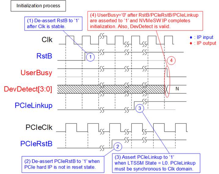
Figure 5: Timing diagram during initialization process
The sequence of the initialization process is as follows.
1) Wait until Clk is stable and then de-asserts RstB to ‘1’ to start IP operation.
2) PCIe hard IP de-asserts PCIeRstB to ‘1’ after finishing PCIe reset sequence. PCIe hard IP is ready to interface with the application layer.
3) Assert PCIeLinkup to ‘1’ after LTSSM state of PCIe hard IP is L0 state. Though LTSSM state is run on PCIeClk, PCIeLinkup must be generated on Clk domain. Asynchronous register must be applied to generate PCIeLinkup. After that, NVMeSW IP starts initialization process.
4) When finishing initialization, NVMeSW IP de-asserts UserBusy to ‘0’. DevDetect[3:0] signal is valid to show the on-line status of four SSDs. If no device is found, DevDetect=”0000” and error flag is asserted to ‘1’. UserBusy is not de-asserted to ‘0’ when no device is detected.
After finishing above sequence, NVMeSW IP is ready to receive the command from user.
Control interface of dgIF typeS
dgIF typeS signals are split into two groups. First group is control interface for sending command with the parameters and monitoring the status. Second group is data interface for transferring data stream in both directions.
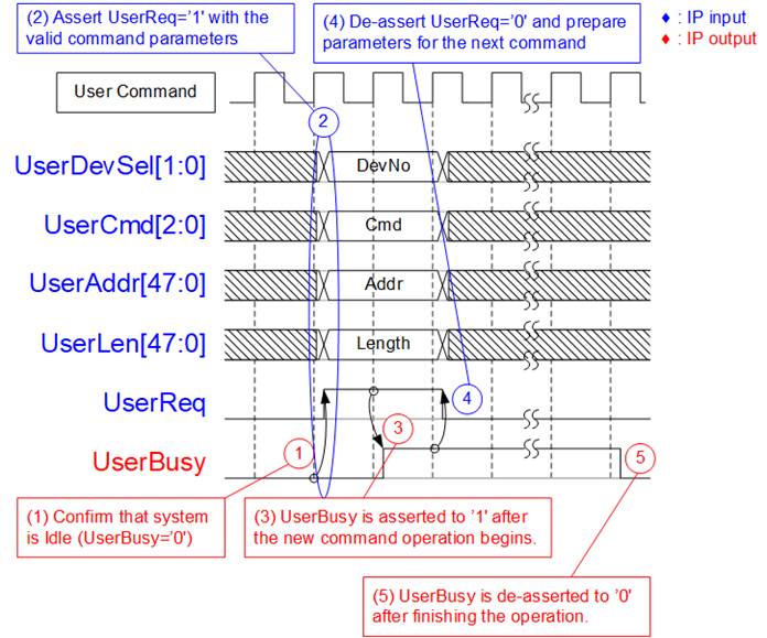
Figure 6: Contol interface of dgIF typeS timing diagram
1) Before sending new command to the IP, UserBusy must be equal to ‘0’ to confirm that IP is the Idle state.
2) Command and the parameters such as UserDevSel, UserCmd, UserAddr and UserLen must be valid when asserting UserReq to ’1’ for sending the new command request.
3) IP asserts UserBusy to ‘1’ after starting the new command operation.
4) After UserBusy is asserted to ‘1’, UserReq is de-asserted to ‘0’ to finish the current request. New parameters for the next command could be prepared on the bus. UserReq for the new command must not be asserted to ‘1’ until the current command operation is finished.
5) UserBusy is de-asserted to ‘0’ after the command operation is completed. New command request could be sent by asserting UserReq to ‘1’.
Note: The number of parameters using in each command is different.
- Write and Read command: Use UserDevSel, UserCmd, UserAddr and UserLen.
- SMART and Flush command: Use UserDevSel, UserCmd and CtmSubmDW0-DW15.
- Identify and Shudown command: Use UserDevSel and UserCmd.
Data interface of dgIF typeS
Data interface of dgIF typeS is applied for transferring data stream when operating Write command or Read command. The interface is compatible to general FIFO interface. 16-bit FIFO read data counter (UserFifoRdCnt) shows total data stored in the FIFO before transferring as a burst. The burst size is 512 bytes or 32 cycles of 128-bit data.
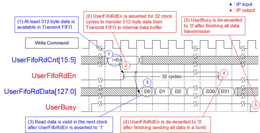
Figure 7: Transmit FIFO Interface for Write command
In Write command, data is read from Transmit FIFO until total data are transferred completely. The details to transfer data are described as follows.
1) Before starting a new burst transfer, UserFifoRdCnt[15:5] is monitored. The IP waits until at least 512-byte data is available in Transmit FIFO (UserFifoRdCnt[15:5] is not equal to 0).
2) The IP asserts UserFifoRdEn to ‘1’ for 32 clock cycles to read 512-byte data from Transmit FIFO.
3) UserFifoRdData is valid in the next clock cycle after asserting UserFifoRdEn to ‘1’. 32 data are continuously transferred.
4) UserFifoRdEn is de-asserted to ‘0’ after reading the 32th data. Repeat step 1) – 4) to transfer the next 512-byte until total data size is equal to the transfer size in the command.
5) After total data is completely transferred, UserBusy is de-asserted to ‘0’.
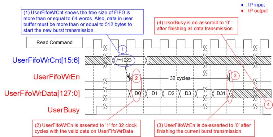
Figure 8: Receive FIFO Interface for Read command
In Read command, data is transferred from SSD to Receive FIFO until total data are completely transferred. The details to transfer data are as follows.
1) Before starting the new burst transmission, UserFifoWrCnt[15:6] is monitored. The IP waits until the free space of Receive FIFO is enough (UserFifoWrCnt[15:6] is not equal to all 1 or 1023). After received data from the SSD is more than or equal to 512 bytes, the new burst transmission begins.
2) The IP asserts UserFifoWrEn to ‘1’ for 32 clock cycles to transfer 512-byte data from the data buffer to user logic.
3) After finishing transferring 512-byte data, UserFifoWrEn is de-asserted to ‘0’. Repeat step 1) – 3) to transfer the next 512-byte data until total data size is equal to the transfer size in the command.
4) After total data is completely transferred, UserBusy is de-asserted to ‘0’.
IdenCtrl/IdenName
It is recommened to send Identify command to the IP as the first command after system boots up. This command updates the necessary information of all SSDs, i.e. total capacity (LBASize0-LBASize3) and LBA unit size (LBAMode[3:0]). The SSD information is applied to be the limitation of the input parameters when operating Write or Read command, described as follows.
1) The sum of the address (UserAddr) and transfer length (UserLen) of Write and Read command must not be more than total capacity (LBASize) of the active SSD.
2) If LBAMode of the active SSD is equal to ‘1’ (LBA unit size is 4 Kbytes), the three lower bit (bit[2:0]) of UserAddr and UserLen must be always equal to ‘0’ to align 4-Kbyte unit.
When multiple SSDs are detected in the system, user logic must send Identify command many times with switching UserDevSel value for operating with all SSDs. After finishing the command, LBASize and LBAMode of all SSDs are updated (not equal to 0). The example to send Identify command to SSD#0 is shown in Figure 9.
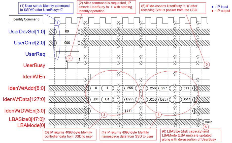
Figure 9: Identify command timing diagram
The details when running Identify command are shown as follows.
1) Set the active SSD (UserDevSel) and send Identify command (UserCmd=”000” and UserReq=’1’).
2) The IP asserts UserBusy to ‘1’ after running Identify command.
3) 4096-byte Identify controller data is returned to user. IdenWrAddr is equal to 0-255 with asserting IdenWrEn. Also, IdenWrData and IdenWrDWEn are valid at the same clock as IdenWrEn=’1’.
4) 4096-byte Identify namespace data is returned. IdenWrAddr is equal to 256-511. IdenWrAddr[8] can be applied to check data type which is Identify controller data or Identify namespace data.
5) UserBusy is de-asserted to ‘0’ after finishing the Identify command.
6) LBASize and LBAMode of the active SSD are simultaneously updated. Change UserDevSel and resend Identify command to the new SSD if some SSDs are not identified.
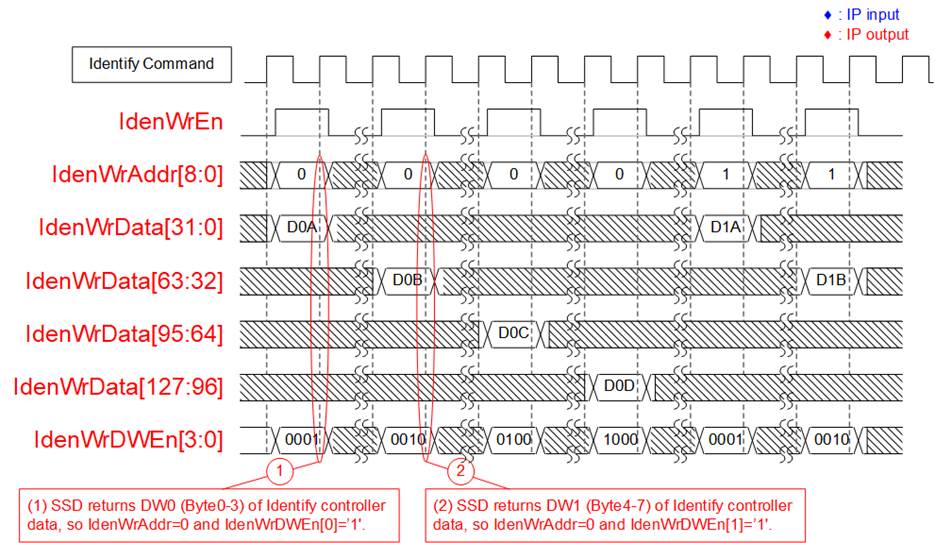
Figure 10: IdenWrDWEn timing diagram
IdenWrDWEn is 4-bit signal to be valid signal of 32-bit data. Some SSDs do not return 4-Kbyte Identify controller data and Identify namespace data continuously, but it returns only one dword (32-bit) at a time. Therefore, one bit of IdenWrDWEn is asserted to ‘1’ in the write cycle to write 32-bit data, as shown in Figure 10. IdenWrDWEn[0], [1], [2] and [3] corresponds to IdenWrData[31:0], [63:32], [95:64] and [127:96] respectively.
Shutdown
Shutdown command is recommended to send as the last command before the system is powered down. When Shutdown command is issued, SSD flushes the data from the internal cache to flash memory. After the command is issued, NVMeSW IP and SSD are not available until the system is powered down. If the SSD is powered down without Shutdown command, the total count of unsafe shutdowns, read by SMART command, is increased.
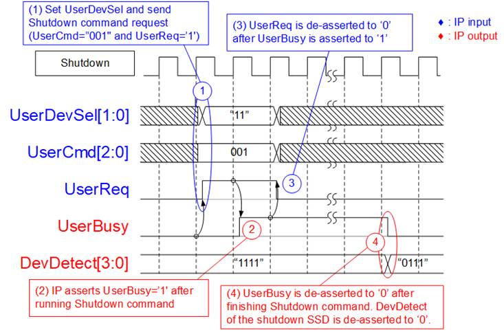
Figure 11: Shutdown command timing diagram
The details when running Shutdown command are shown as follows.
1) Before sending the command request, the IP must be in the Idle state (UserBusy=’0’). To send Shutdown command, UserDevSel is set to select the SSD and UserCmd is set to “001”. UserReq is asserted to ‘1’ with the stable value on UserDevSel and UserCmd.
2) UserBusy is asserted to ‘1’ after NVMeSW IP runs Shutdown command.
3) UserReq is de-asserted to ‘0’ to clear the current request. Next, user logic can change the value of UserDevSel and UserCmd for the next command request.
4) UserBusy is de-asserted to ‘0’ when the selected SSD is completely shut down. DevDetect of selected SSD is de-asserted to ‘0’. The example of shutdown command is shown in Figure 11. DevDetect[0] changes to ‘0’ after SSD#0 (UserDevSel=”00”) completes Shutdown operation. After that, user cannot send the command request to SSD#0.
SMART
SMART command is applied to check the SSD health. After sending SMART command, 512-byte health information is returned from the SSD. SMART command loads the parameters from CtmSubmDW0-DW15 signals on Custom command interface. User sets 16-dword data as constant value for SMART command. After that, the SMART data is returned via CtmRAM port as shown in Figure 12.
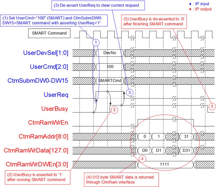
Figure 12: Example to send SMART command
The details when running SMART command are shown as follows.
1) Before sending the command request, the IP must be in the Idle state (UserBusy=’0’).
All input parameters must be stable when UserReq is asserted to ‘1’ for sending the request.
CtmSubmDW0-DW15 is set as constant value by following value for SMART command.
CtmSubmDW0 = 0x0000_0002
CtmSubmDW1 = 0xFFFF_FFFF
CtmSubmDW2 – CtmSubmDW5 = 0x0000_0000
CtmSubmDW6 = 0x2000_0000
CtmSubmDW7 – CtmSubmDW9 = 0x0000_0000
CtmSubmDW10 = 0x007F_0002
CtmSubmDW11 – CtmSubmDW15 = 0x0000_0000
2) Assert UserBusy to ‘1’ after NVMeSW IP runs SMART command.
3) UserReq is de-asserted to ‘0’ to clear the current request. Next, user logic can change the input parameters for the next command request.
5) UserBusy is de-asserted to ‘0’ when finishing SMART command.
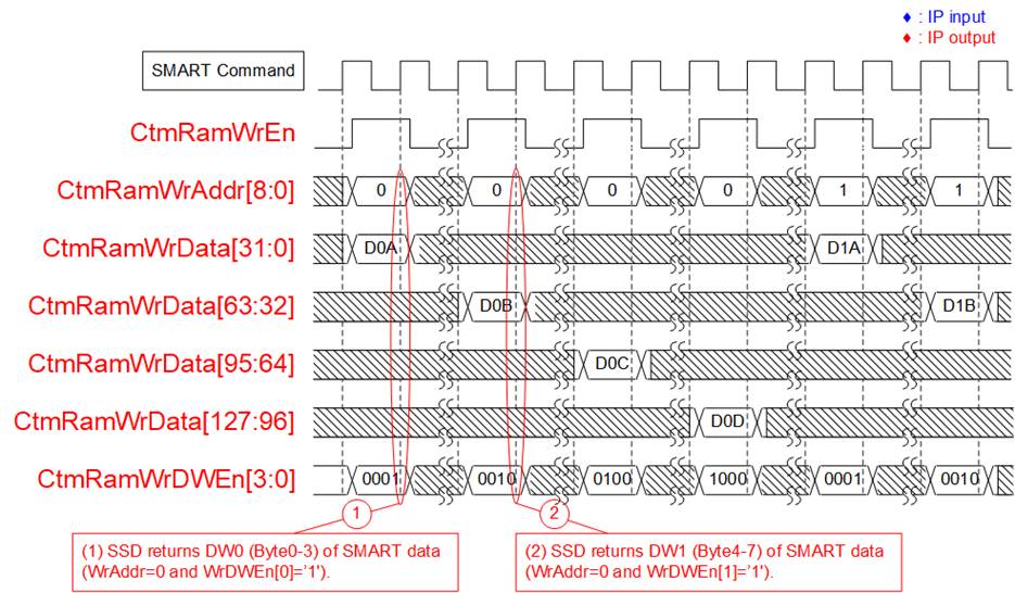
Figure 13: CtmRamWrDWEn timing diagram
Similar to Identify command, some SSDs do not return 512-byte data continuously but returns only one dword (32-bit) at a time. Therefore, one bit of CtmRamWrDWEn is asserted to ‘1’ in the write cycle to be the valid signal of 32-bit CtmRamWrData. CtmRamWrDWEn[0], [1], [2] and [3] corresponds to CtmRamWrData[31:0], [63:32], [95:64] and [127:96] respectively.
Flush
Most SSDs accelerate write performance by storing write data to cache before flushing to the flash memory by the SSD controller. If power is down unexpectedly, the data in the cache may be lost and not stored to the flash memory. Flush command is the command to force the SSD controller to flush data from the cache. After sending Flush command, all data in previous Write command can be guaranteed.
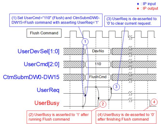
Figure 14: Flush command timing diagram
The details for running Flush command are shown as follows.
1) Before sending the command request, the IP must be in the Idle state (UserBusy=’0’).
All input parameters must be stable when UserReq is asserted to ‘1’ for sending the request.
CtmSubmDW0-DW15 is set as constant value by following value for Flush command.
CtmSubmDW0 = 0x0000_0000
CtmSubmDW1 = 0x0000_0001
CtmSubmDW2 – CtmSubmDW15 = 0x0000_0000
2) UserBusy is asserted to ‘1’ after NVMeSW IP runs Flush command.
3) UserReq is de-asserted to ‘0’ to clear the current request. Next, user logic can change the input parameters for the next command request.
4) UserBusy is de-asserted to ‘0’ when finishing Flush command.
Error
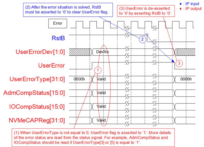
Figure 15: Error flag timing diagram
When the error is found during running initialization process or operating some commands, UserError flag is asserted to ‘1’. UserErrorType is read to check the error type. NVMeCAPReg, AdmCompStatus and IOCompStatus are valid for monitoring error details after UserError is asserted to ‘1’.
When the error is found during running initialization process, it is recommended to read NVMeCAPReg to check capability of NVMe SSD. When the error is found during operating the command, it is recommended to read AdmCompStatus or IOCompStatus, depending on the command type, which is decoded from the received packet.
UserError flag is cleared by RstB signal only. After the failure is solved, RstB is asserted to ‘0’ to clear the error flag.
Verification Methods
The NVMeSW IP Core functionality was verified by simulation and also proved on real board design by using Arria10 GX Development board.
Recommended Design Experience
Experience design engineers with a knowledge of QuartusII Tools should easily integrate this IP into their design.
Ordering Information
This product is available directly from Design Gateway Co., Ltd. Please contact Design Gateway Co., Ltd. For pricing and additional information about this product using the contact information on the front page of this datasheet.
Revision History
|
Revision |
Date |
Description |
|
1.0 |
29-Apr-2019 |
Initial release |
|
1.1 |
13-Feb-2020 |
Support AB18 |
|
1.2 |
12-Oct-2020 |
Update company info |