
Design Gateway Co., Ltd
E-mail: ip-sales@design-gateway.com
URL: design-gateway.com
Features
· Function as an NVMe host engine for direct NVMe SSD access without the need for a CPU or external memory
· Two Data buffer modes: High-speed (1 MB RAM) or Small-memory (256 KB RAM)
· Simple user interface through dgIF typeS
· Support seven commands: Identify, Shutdown, Write, Read, SMART, Secure Erase, and Flush
· Supported NVMe device specifications:
· Base Class Code: 01h (mass storage)
· Sub Class code: 08h (Non-volatile)
· Programming Interface: 02h (NVMHCI)
· Memory Page Size Minimum (MPSMIN): 0 (4KB)
· Maximum Data Transfer Size (MDTS): At least 5 (128 KB) or 0 (no limitation)
· Maximum Queue Entries Support (MQES): At least 15
· LBA unit: 512 bytes or 4 KB
· User clock frequency: At least the PCIe clock frequency (250 MHz for Gen4)
· PCIe Gen4 Hard IP interface: 256-bit AXI4-Stream bus
· Available reference design using AB17-M2FMC adapter board:
· 1-ch demo on Atum A5 Development Kit
· Customized services available for implementing additional NVMe commands, such as TRIM and Sanitize, or for modifying the RAM size
Applications
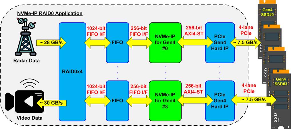
Figure 1 NVMe-IP Application
The NVMe IP Core for Gen4, integrated with GTS AXI Streaming PCIe IP (PCIe Hard IP) from Altera provides an efficient solution for accessing NVMe Gen4 SSDs without requiring a CPU or external memory (DDR). With embedded memory blocks of 1 MB / 256 KB, the NVMe-IP meets the demands of applications that require large storage capacity combined with high-throughput data transfer. The PCIe Hard IP is configured as a 4-lane PCIe Gen4 interface, allowing for direct connection to NVMe Gen4 SSDs.
Using the NVMe-IP, the achievable data throughput for a single NVMe Gen4 SSD is approximately 7.5 GB/s. To further increase transfer performance, a RAID0 architecture can be implemented by deploying multiple NVMe-IPs in parallel with multiple PCIe Hard IPs, as illustrated in Figure 1. For example, a four-channel RAID0 configuration using four NVMe-IPs and four NVMe SSDs can scale the aggregate throughput to approximately 28 GB/s for write operations and 30 GB/s for read operations. This architecture is well suited for applications such as radar data acquisition, high-resolution video processing, and other systems requiring sustained high-speed data streaming.
In addition to the standard NVMe-IP, Design Gateway provides specialized NVMe IP cores optimized for specific application requirements:
Multiple User NVMe IP Core – Enables multiple users to access an NVMe SSD for high-performance write and read operations simultaneously.
https://dgway.com/muNVMe-IP_A_E.html
Random Access by Multiple User NVMe IP Core – Enables simultaneous write/read access by two users to the same SSD. Optimized for high random-access performance in systems with non-contiguous data access patterns.
https://dgway.com/rmNVMe-IP_A_E.html
NVMe IP Core for PCIe Switch – Enable access to multiple NVMe SSDs through a PCIe switch, effectively scaling storage capacity and supporting shared high-speed access.
https://dgway.com/NVMe-IP_A_E.html
NVMe IP Core with PCIe Soft IP – Provides NVMe SSD access without relying on PCIe Hard IP.
https://dgway.com/NVMeG4-IP_A_E.html
General Description
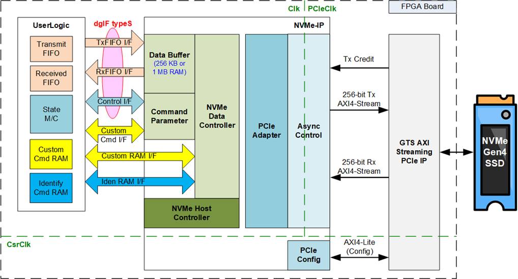
Figure 2 NVMe-IP for Gen4 Block Diagram
The NVMe-IP for Gen4 is a complete host controller solution that enables access to an NVMe Gen4 SSD using the NVM Express standard. The physical interface for the NVMe SSD is PCIe, and the lower layer hardware is implemented using GTS AXI Streaming PCIe IP from Altera (PCIe Hard IP).
The NVMe IP core implements seven NVMe commands, including Identify, Shutdown, Write, Read, SMART, Secure Erase, and Flush, and utilizes two user interface groups to transfer commands and data. The Control interface is used for transferring commands and their parameters, while the Data interface is used for transferring data when required by the command. For Write/Read commands, the Control interface and Data interface use dgIF typeS, which is our standard interface for the storage. The Control interface of dgIF typeS includes start address, transfer length, and request signals, and the Data interface uses the standard FIFO interface.
The SMART, Secure Erase, and Flush are Custom commands that use the Custom Cmd I/F for control path and Custom RAM I/F for data path. Meanwhile, the Identify command uses its own data interface – Iden RAM I/F, and the same Control interface as Write or Read command, as shown in Figure 2.
If abnormal conditions are detected during initialization or certain command operation, the NVMe-IP may assert an error signal. The error status can be read from the IP for more details. Once the error cause is resolved, both the NVMe-IP and SSD must be reset.
To ensure continuous packet transmission until the end of the packet on the user interface of PCIe Hard IP, the user logic clock frequency must be equal to or greater than the PCIe clock frequency (250 MHz). This requires that data is valid every clock cycle between the start and the end of the frame. This user clock frequency limitation can guarantee that the bandwidth on the user interface is equal to or greater than PCIe Hard IP bandwidth.
Overall, the NVMe-IP provides a comprehensive solution for accessing NVMe SSDs. The IP core comes with reference designs on FPGA evaluation boards, allowing users to assess functionality and performance prior to purchase. These reference designs are available for evaluation before deployment.
Functional Description
The NVMe-IP operation is divided into three phases: Initialization, Command Operation, and Inactive State, as shown in Figure 3. Upon de-asserting the IP reset, the initialization phase begins. Once all PCIe and NVMe registers are successfully configured during initialization, the IP transitions to the Command Operation phase.
In the Command Operation phase, the user should first execute the Identify command to verify device status and retrieve device capacity. Afterward, other commands—including Write, Read, SMART, Secure Erase, and Flush—can be issued. Before powering down the system, it is recommended to execute the Shutdown command to ensure data integrity and proper SSD power-down sequence.
Further details of the IP operation in these three phases are described below.
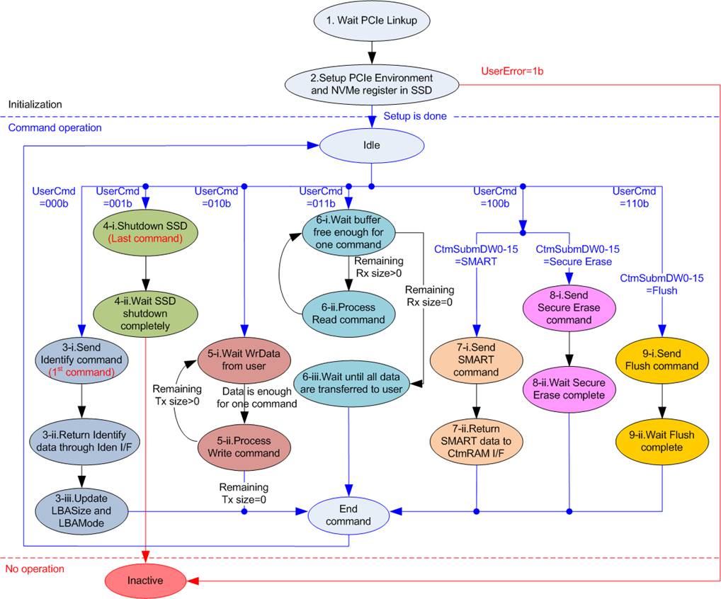
Figure 3 NVMe-IP Operation Flow
The operational sequence of the NVMe-IP can be outlined in the following steps.
1) The IP waits for PCIe to be ready by monitoring the Linkup status from the PCIe Hard IP.
2) The IP begins the initialization process by setting up flow control and configuring PCIe and NVMe registers. Upon successful completion of the initialization, the IP transitions to the Idle state, where it awaits new command request from the user. If any errors are detected during the initialization process, the IP switches to the Inactive state, with UserError set to 1b.
3) The first command from the user must be the Identify command (UserCmd=000b), which updates the LBASize (disk capacity) and LBAMode (LBA unit=512 bytes or 4 KB).
4) The last command before powering down the system must be the Shutdown command (UserCmd=001b). This command is recommended to guarantee the SSD is powered down in a proper sequence. Without the Shutdown command, the write data in the SSD cannot be guaranteed. After the Shutdown command completion, both the NVMe-IP and SSD change to the Inactive state, and no new command can be executed until the IP is reset.
i) The IP waits until sufficient user write data is available for one command (128 KB, or smaller for the last portion).
ii) The IP sends the Write command to the SSD. If data remains, the process returns to step (5i). Otherwise, the IP waits for the completion status for all issued Write commands and then returns to the Idle state.
i) The IP checks whether one of the following completion conditions is met:
· Data remaining: The IP waits until sufficient space is available in the Data buffer for one command (128 KB, or the remaining size for the last loop), and then proceeds to step (6ii).
· No data remaining: The IP proceeds directly to step (6iii).
ii) The IP sends the Read command to the SSD and then returns to step (6i).
iii) The IP waits until all read data has been transferred from the Data buffer to user logic, and then returns to the Idle state. Upon completion, the Data buffer is empty.
7) When executing a SMART command (UserCmd=100b, CtmSubmDW0-15=SMART), the IP proceeds as follows:
i) The IP sends a Get Log Page command to retrieve SMART/Health information from the SSD.
ii) The SSD returns 512 bytes of data, which the IP forwards via the Custom RAM I/F (CtmRamAddr=00h–0Fh).
8) When executing a Secure Erase command (UserCmd=100b, CtmSubmDW0-15=Secure Erase), the IP proceeds as follows:
i) The IP sends the Secure Erase command to the SSD.
ii) The IP waits for status confirmation of completion from the SSD.
9) When executing a Flush command (UserCmd=110b, CtmSubmDW0-15=Flush), the IP proceeds following steps:
i) The IP sends the Flush command to the SSD.
ii) The IP waits for status confirmation of completion from the SSD.
To design the host engine for NVMe SSD, NVMe-IP implements two protocols: NVMe and PCIe. The NVMe protocol is used to interface with the user, while the PCIe protocol is used to interface with PCIe Hard IP. Figure 2 shows the hardware inside the NVMe-IP which is split into two groups, NVMe and PCIe.
NVMe
The NVMe group supports seven commands, which are split into two categories - Admin commands and NVM commands. Admin commands include Identify, Shutdown, SMART, and Secure Erase, while NVM commands include Write, Read, and Flush. After executing a command, the status returned from the SSD is latched either to AdmCompStatus (for status returned from Admin commands) or IOCompStatus (for status returned from NVM commands), depending on the command type.
The parameters of Write or Read command are configured through the Control interface of dgIF typeS, while the parameters of SMART, Secure Erase, or Flush command are set by CtmSubmDW0-15 of the Custom Cmd I/F. Data for Write or Read command is transferred using the FIFO interface, a part of dgIF typeS. The data for Write and Read commands is stored in the IP’s Data buffer. For other command types, the Data interface utilizes distinct interfaces - Iden RAM I/F for the Identify command and Custom RAM I/F for the SMART command.
Further details of each submodule are described as follows.
· NVMe Host Controller
The NVMe Host Controller serves as the core controller within the NVMe-IP. It operates in two phases: the initialization phase and the command operation phase. The initialization phase runs once when the system is booted up, for configuring the NVMe register within the SSD. Once the initialization phase is completed, it enters the command operation phase. During this phase, the controller controls the sequence of transmitted and received packets for each command.
To initiate the execution of each command, the command parameters are stored in the Command Parameter, facilitating packet creation. Subsequently, the packet is forwarded to the PCIe Adapter for converting NVMe packets into PCIe packets. After each command operation is executed, a status packet is received from the SSD. The controller decodes the status value, verifying whether the operation was completed successfully or an error occurred. In cases where the command involves data transfer, such as Write or Read command, the controller must handle the order of data packets, which are created and decoded by the NVMe Data controller.
· Command Parameter
The Command Parameter module creates the command packet sent to the SSD and decodes the status packet returned from the SSD. The inputs and outputs of this module are controlled by the NVMe Host Controller. Typically, a command consists of 16 Dwords (1 Dword = 32 bits). When executing Identify, Shutdown, Write, and Read commands, all 16 Dwords are created by the Command parameter module, which are initialized by the user inputs on dgIF typeS. When executing SMART, Secure Erase, and Flush commands, all 16 Dwords are directly loaded via CtmSubmDW0-CtmSubmDW15 of Custom Cmd I/F.
· Data Buffer
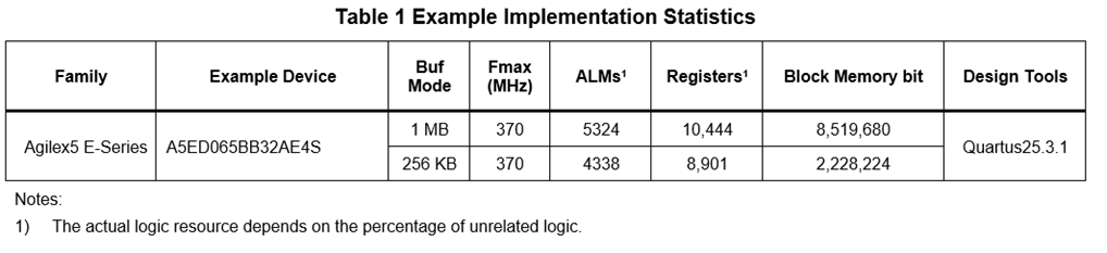
The Data Buffer supports two modes: High-speed mode, which uses 1 MB of RAM, and Small-memory mode, which uses 256 KB of RAM. The RAM is implemented using memory blocks. The buffer temporarily stores data transferred between the UserLogic and the SSD during Write and Read command operations.
· NVMe Data Controller
The NVMe Data Controller module is used when the command must transfer data such as Identify, SMART, Write, and Read. This module manages three data interfaces for transferring with the SSD.
- FIFO Interface: Used with the Data buffer during the execution of Write or Read commands.
- Custom RAM Interface: Used when executing SMART command.
- Identify Interface: Used when executing Identify command.
The NVMe Data Controller is responsible for creating and decoding of data packets. Similar to the Command Parameter module, the input and output signals of the NVMe Data Controller module are controlled by the NVMe Host Controller.
PCIe
The PCIe protocol is the outstanding low-layer protocol for the high-speed application, and the NVMe protocol runs over it. Therefore, the NVMe layer can be operated after the PCIe layer completes the initialization. Three modules are designed to support the PCIe protocol – PCIe Config, PCIe Adapter, and Async Control. Additional details of these modules are provided below.
· PCIe Config
During initialization process, the PCIe Config sets up the PCIe environment of the SSD via the AXI4-Lite interface.
· PCIe Adapter
After the PCIe Config completes the PCIe environment setup, the PCIe Adapter converts command and data packets from the NVMe module into PCIe packets through a 256-bit Tx AXI4-Stream interface. It also performs the reverse conversion for incoming PCIe packets through a 256-bit Rx AXI4-Stream interface. The data flow on the Tx AXI4-Stream interface is controlled by the Tx Credit port.
· Async Control
Async Control incorporates asynchronous registers and buffers designed to facilitate clock domain crossing. The user clock frequency must match or exceed the PCIe clock frequency to ensure sufficient bandwidth for continuous packet data transmission. The majority of the logic within the NVMe-IP operates in the user clock domain, while the PCIe Hard IP operates in the PCIe clock domain.
User Logic
The user logic can be implemented using a small state machine responsible for sending commands along with their corresponding parameters. For instance, simple registers are used to specify parameters for Write or Read command, such as address and transfer size. Two separate FIFOs are connected to manage data transfer for Write and Read commands independently.
When executing the SMART and Identify commands, each data output interface connects to 2-Port RAM (one read port and one write port) with byte enable capability. Both the FIFO and RAM have a data width of 256 bits, while their memory depth can be configured to different values. Specifically, the data size for the Identify command is 8 KB, while the SMART command has a data size of 512 bytes.
PCIe Hard IP from Altera (GTS AXI Streaming IP for PCIe)
The PCIe Hard IP on Agilex5, also known as GTS AXI Streaming IP for PCIe, is used to interface with the NVMe-IP through four key connections. These include the AXI4-ST Tx Port for transmitting packets, the AXI4-ST Rx Port for receiving PCIe packets, the Tx Credit Port for managing transmit flow control, and the AXI4-Lite interface for configuring PCIe settings.
This Hard IP implements the Transaction layer, Data Link layer, and Physical layer of the PCIe protocol. The number of NVMe SSDs that can be connected to a single FPGA device is limited by the number of available PCIe Hard IP blocks on that FPGA. More comprehensive details about GTS AXI Streaming IP for PCIe can be found in the documentation at the following link:
https://docs.altera.com/r/docs/813754/current
Additionally, the IP requires a specific reset sequence, which must be implemented as described in the following Altera document:
This reset sequencer is provided as HDL code as part of the NVMe-IP for Gen4 reference design included in the IP deliverables.
Core I/O Signals
Table 2 provides detailed descriptions of configurable parameters, while Table 3 - Table 5 outline the I/O signals for NVMe-IP.
Table 2 Core Parameters
|
Name |
Value |
Description |
|
BufMode |
0 or 1 |
Data buffer mode. 1: High-speed mode using 1 MB buffer. 0: Small-memory mode using 256 KB buffer. |
Table 3 User I/O Signals (Synchronous with Clk)
|
Signal name |
Dir |
Description |
|
Control I/F of dgIF typeS |
||
|
RstB |
In |
Synchronous reset. Active low. It should be de-asserted to 1b when the Clk signal is stable. |
|
Clk |
In |
User clock for running the NVMe-IP. The frequency of this clock must be equal to or greater than the PCIeClk frequency, which is the clock output from the PCIe Hard IP. For 4-lane PCIe Gen4, the PCIeClk frequency is 250 MHz. |
|
UserCmd[2:0] |
In |
User Command. Valid when UserReq=1b. The possible values are 000b: Identify, 001b: Shutdown, 010b: Write SSD, 011b: Read SSD, 100b: SMART/Secure Erase, 110b: Flush, Others: Reserved. |
|
UserAddr[47:0] |
In |
The start address to write/read from the SSD in 512-byte units. Valid when UserReq=1b. If the LBA unit = 4 KB, UserAddr[2:0] must always be set to 000b to align with 4 KB unit. If the LBA unit = 512 bytes, it is recommended to set UserAddr[2:0]=000b to align with 4 KB size (SSD page size). The 4KB address unalignment results in reduced write/read performance for most SSDs. |
|
UserLen[47:0] |
in |
The total transfer size to write/read from the SSD in 512-byte units. Valid from 1 to (LBASize-UserAddr). If the LBA unit = 4 KB, UserLen[2:0] must always be set to 000b to align with the 4 KB unit. This parameter is applicable when UserReq=1b. |
|
UserReq |
In |
Set to 1b to initiate a new command request and reset to 0b after the IP starts the operation, signaled by setting UserBusy to 1b. This signal can only be asserted when the IP is in the Idle state (UserBusy=0b). Command parameters, including UserCmd, UserAddr, UserLen, and CtmSubmDW0-DW15, must maintain their values during UserReq set to 1b. UserAddr and UserLen are inputs for Write/Read commands while CtmSubmDW0-DW15 are inputs for SMART, Secure Erase, or Flush command. |
|
UserBusy |
Out |
Set to 1b when the IP is busy. New request must not be sent (UserReq=1b) when the IP is busy. |
|
LBASize[47:0] |
Out |
The total capacity of the SSD in 512-byte units. Default value is 0. This value is valid after the Identify command is completed. |
|
LBAMode |
Out |
The LBA unit size of the SSD (0b: 512 bytes, 1b: 4 KB). Default value is 0b. This value is valid after the Identify command is completed. |
|
UserError |
Out |
Error flag. Asserted to 1b when the UserErrorType is not equal to 0. The flag is cleared to 0b by asserting RstB to 0b. |
|
Signal name |
Dir |
Description |
|
Control I/F of dgIF typeS |
||
|
UserErrorType[31:0] |
Out |
Error status. [0] – An error when PCIe class code is incorrect. [1] – An error from Controller capabilities (CAP) register, which can occur due to various reasons. - Memory Page Size Minimum (MPSMIN) is not equal to 0. - NVM command set flag (bit 37 of CAP register) is not set to 1. - Doorbell Stride (DSTRD) is not equal to 0. - Maximum Queue Entries Supported (MQES) is less than 15. More details of each register can be found in the NVMeCAPReg signal. [2] – An error when the Admin completion entry is not received within the specified timeout. [3] – An error when the status register in the Admin completion entry is not 0 or when the phase tag/command ID is invalid. Further information can be found in the AdmCompStatus signal. [4] – An error when the IO completion entry is not received within the specified timeout. [5] – An error when the status register in the IO completion entry is not 0 or when the phase tag is invalid. More details are available in the IOCompStatus signal. [6] – An error from unsupported LBA unit (not equal to 512 bytes or 4KB). [7] – An error when configuration interface response is not successful. [8] – An error when the received size of Transaction Layer Packet (TLP) is incorrect. [9] – Reserved. Bit[15:10] are mapped to Uncorrectable Error Status Register. [10] – Mapped to Unsupported Request (UR) Status (bit[20]). [11] – Mapped to Completer Abort (CA) Status (bit[15]). [12] – Mapped to Unexpected Completion Status (bit[16]). [13] – Mapped to Completion Timeout Status (bit[14]). [14] – Mapped to Poisoned TLP Received Status (bit[12]). [15] – Mapped to ECRC Error Status (bit[19]). [23:16] – Reserved. Bit[30:24] are also mapped to Uncorrectable Error Status Register. [24] – Mapped to Data Link Protocol Error Status (bit[4]). [25] – Mapped to Surprise Down Error Status (bit[5]). [26] – Mapped to Receiver Overflow Status (bit[17]). [27] – Mapped to Flow Control Protocol Error Status (bit[13]). [28] – Mapped to Uncorrectable Internal Error Status (bit[22]). [29] – Mapped to Malformed TLP Status (bit[18]). [30] – Mapped to ACS Violation Status (bit[21]). [31] – Reserved. Note: Timeout period of bit[2]/[4] is determined by the TimeOutSet input. |
|
Data I/F of dgIF typeS |
||
|
UserFifoWrCnt[15:0] |
In |
Write data counter for the Receive FIFO. Used to monitor the FIFO full status. When the FIFO becomes full, data transmission from the Read command temporarily halts. If the data count of FIFO is less than 16 bits, the upper bits should be padded with 1b to complete the 16-bit count. |
|
UserFifoWrEn |
Out |
Asserted to 1b to write data to the Receive FIFO when executing the Read command. |
|
UserFifoWrData[255:0] |
Out |
Write data bus of the Receive FIFO. Valid when UserFifoWrEn=1b. |
|
UserFifoRdCnt[15:0] |
In |
Read data counter for the Transmit FIFO. Used to monitor the amount of data stored in the FIFO. If the counter indicates an empty status, the transmission of data packets for the Write command temporarily pauses. When the data count of FIFO is less than 16 bits, the upper bits should be padded with 0b to complete the 16-bit count. Note: For current NVMe-IP operation, the latency between UserFifoRdCnt[15:0] and UserFifoRdEn must be exactly 1 clock cycle. If the system requires additional latency, please contact us for customized adapter logic. |
|
UserFifoEmpty |
In |
Unused for this IP. |
|
UserFifoRdEn |
Out |
Asserted to 1b to read data from the Transmit FIFO when executing the Write command. |
|
UserFifoRdData[255:0] |
In |
Read data returned from the Transmit FIFO. Valid in the next clock after UserFifoRdEn is asserted to 1b. |
|
Signal name |
Dir |
Description |
|
NVMe-IP Interface |
||
|
IPVersion[31:0] |
Out |
IP version number. |
|
TestPin[31:0] |
Out |
Reserved as the IP Test point. |
|
TimeOutSet[31:0] |
In |
Timeout value to wait for completion from SSD. The time unit is equal to 1/(Clk frequency). When TimeOutSet is equal to 0, Timeout function is disabled. |
|
AdmCompStatus[15:0] |
Out |
Status output from Admin Completion Entry. [0] – Set to 1b when the Phase tag or Command ID in Admin Completion Entry is invalid. [15:1] – Status field value of Admin Completion Entry |
|
IOCompStatus[15:0] |
Out |
Status output from IO Completion Entry [0] – Set to 1b when Phase tag in IO Completion Entry is invalid. [15:1] – Status field value of IO Completion Entry |
|
NVMeCAPReg[31:0] |
Out |
The parameter value of the NVMe capability register when UserErrorType[1] is asserted to 1b. [15:0] – Maximum Queue Entries Supported (MQES) [19:16] – Doorbell Stride (DSTRD) [20] – NVM command set flag [24:21] – Memory Page Size Minimum (MPSMIN) [31:25] – Undefined |
|
Identify Interface |
||
|
IdenWrEn |
Out |
Asserted to 1b for sending data output from Identify command. |
|
IdenWrDWEn[7:0] |
Out |
Dword (32-bit) enable of IdenWrData. Valid when IdenWrEn=1b. 1b: This Dword data is valid, 0b: This Dword data is not available. Bit[0], [1], …, [7] correspond to IdenWrData[31:0], [63:32], …, [255:224], respectively. |
|
IdenWrAddr[7:0] |
Out |
Index of IdenWrData in 256-bit unit. Valid when IdenWrEn=1b. 00h-7Fh: 4KB Identify controller data, 80h-FFh: 4KB Identify namespace data. |
|
IdenWrData[255:0] |
Out |
4KB Identify controller data or Identify namespace data. Valid when IdenWrEn=1b. |
|
Custom Interface (Command and RAM) |
||
|
CtmSubmDW0[31:0] – CtmSubmDW15[31:0] |
In |
16 Dwords of Submission queue entry for SMART, Secure Erase, or Flush command. DW0: Command Dword0, DW1: Command Dword1, …, and DW15: Command Dword15. These inputs must maintain their values during UserReq set to 1b and UserCmd=100b (SMART/Secure Erase) or 110b (Flush). |
|
CtmCompDW0[31:0] – CtmCompDW3[31:0] |
Out |
4 Dwords of Completion queue entry, output from SMART, Secure Erase, or Flush command. DW0: Completion Dword0, DW1: Completion Dword1, …, and DW3: Completion Dword3. |
|
CtmRamWrEn |
Out |
Asserted to 1b for sending data output from Custom command such as SMART command. |
|
CtmRamWrDWEn[7:0] |
Out |
Dword (32 bits) enable of CtmRamWrData. Valid when CtmRamWrEn=1b. 1b: This Dword data is valid, 0b: This Dword data is not available. Bit[0], [1], …, [7] correspond to CtmRamWrData[31:0], [63:32], …, [255:224], respectively. |
|
CtmRamAddr[7:0] |
Out |
Index of CtmRamWrData when SMART data is received. Valid when CtmRamWrEn=1b. (Optional) Index to request data input through CtmRamRdData for customized Custom commands. |
|
CtmRamWrData[255:0] |
Out |
512-byte data output from SMART command. Valid when CtmRamWrEn=1b. |
|
CtmRamRdData[255:0] |
In |
(Optional) Data input for customized Custom commands. |
Table 4 Physical I/O Signals for PCIe Hard IP (Synchronous to PCIeClk)
|
Signal name |
Dir |
Description |
|
Clock and Reset |
||
|
PCIeRstB |
In |
Synchronous reset signal. Active low. De-assert to 1b when PCIe Hard IP is not in reset state. |
|
PCIeClk |
In |
Clock output from PCIe Hard IP (250 MHz for 4-lane PCIe Gen4) |
|
Transmit Flow Control Credit Interface |
||
|
TxCreditValid |
In |
Asserted to 1b to indicate that TxCreditData is valid. |
|
TxCreditData[18:0] |
In |
Credit limit information and type of transmit credit. [15:0] – Credit limit value. [18:16] – Credit type, defined as follows. 000b: Posted Header Credit, 001b: Non-Posted Header Credit, 010b: Completion Header, 011b: Reserved, 100b: Posted Data Credit, 101b: Non-Posted Data Credit, 110b: Completion Data Credit, 111b: Reserved |
|
PCIe Hard IP Rx Interface |
||
|
PCIeRxReady |
Out |
Asserted to 1b to indicate that NVMe-IP is ready to accept data. Data is transferred when both PCIeRxValid and PCIeRxReady are asserted in the same clock cycle. |
|
PCIeRxValid |
In |
Asserts to 1b to indicate that PCIeRxData is valid. |
|
PCIeRxKeep[31:0] |
In |
Bit[i] indicates that byte[i] of PCIeRxData contains valid data. |
|
PCIeRxData[255:0] |
In |
Receive data bus. Valid when PCIeRxValid is asserted to 1b. |
|
PCIeRxEOP |
In |
Asserts to 1b to indicate that this is the last cycle of the TLP. Valid when PCIeRxValid is asserted to 1b. |
|
PCIeRxHdValid |
In |
Asserts to 1b to indicate that PCIeRxHd is valid. |
|
PCIeRxHd[255:0] |
In |
Receive header data. Valid when PCIeRxHdValid is asserted to 1b. |
|
PCIe Hard IP Tx Interface |
||
|
PCIeTxReady |
In |
Asserts to 1b to indicate that PCIe Hard IP is ready to accept data. Data is transferred when both PCIeTxValid and PCIeTxReady are asserted in the same clock cycle. |
|
PCIeTxValid |
Out |
Asserted to 1b to indicate that PCIeTxData is valid. The NVMe-IP maintains this signal asserted throughout the transmission of a TLP. |
|
PCIeTxKeep[31:0] |
Out |
Bit[i] indicates that byte[i] of PCIeTxData contains valid data. |
|
PCIeTxData[255:0] |
Out |
Data for transmission. Valid when PCIeTxValid is asserted to 1b. |
|
PCIeTxEOP |
Out |
Asserted to 1b to indicate the last cycle of a TLP. Valid when PCIeTxValid is asserted to 1b. |
|
PCIeTxHdValid |
Out |
Asserted to 1b to indicate that PCIeTxHd is valid. |
|
PCIeTxHd[255:0] |
Out |
Header data for transmission. Valid when PCIeTxHdValid is asserted to 1b. |
Table 5 PCIe Hard IP Control and Status Responder Interface (Synchronous to CsrClk)
|
Signal name |
Dir |
Description |
|
System and Link status signal |
||
|
CsrRstB |
In |
Synchronous reset signal. Active low. De-assert this signal to 1b when the PCIe Hard IP is not in reset state. |
|
CsrClk |
In |
The frequency of CsrClk is recommended to be between 100MHz and 250MHz. |
|
PCIeLinkup |
In |
Asserted to 1b when LTSSM state of the PCIe Hard IP is in L0 State. |
|
LinkSpeed[2:0] |
Out |
Negotiated PCIe link speed that is read out from the PCIe Hard IP Configuration Space. 000b: Undefined, 001b: Gen1, 010b: Gen2, 011b: Gen3, 100b: Gen4, Others: Reserved This register is valid after the NVMe-IP has finished initialization (UserBusy=0b). |
|
LinkWidth[2:0] |
Out |
Negotiated PCIe link width that is read out from the PCIe Hard IP Configuration Space. 000b: Undefined, 001b: x1 lane, 010b: x2 lane, 100b: x4 lane. This register is valid after the NVMe-IP has finished initialization (UserBusy=0b). |
|
Control and Status Responder Interface |
||
|
CsrAwValid |
Out |
Asserted to 1b to indicate that CsrAwAddr is valid. |
|
CsrAwReady |
In |
Asserted to 1b to indicate that a transfer on CsrAwAddr can be accepted. |
|
CsrAwAddr[19:0] |
Out |
The address of the first transfer in a write transaction. |
|
CsrwValid |
Out |
Asserted to 1b to indicate that CfgWrData is valid. |
|
CsrwReady |
In |
Asserted to 1b to indicate that a transfer on CfgWrData can be accepted. |
|
CsrwData[31:0] |
Out |
Write data. |
|
CsrwStrb[3:0] |
Out |
Bit[i] indicates that byte[i] of CsrwData holds valid data. |
|
CsrbValid |
In |
Asserted to 1b to indicate that CsrbResp is valid. |
|
CsrbReady |
Out |
Asserted to 1b to indicate that a transfer on CsrbResp can be accepted. |
|
CsrbResp[1:0] |
In |
Write response to indicate the status of a write transfer. |
|
CsrArValid |
Out |
Asserted to 1b to indicate that CsrArAddr is valid. |
|
CsrArReady |
In |
Asserted to 1b to indicate that a transfer on CsrArAddr can be accepted. |
|
CsrArAddr[19:0] |
Out |
The address of the first transfer in a read transaction. |
|
CsrrValid |
In |
Asserted to 1b to indicate that CsrrData is valid. |
|
CsrrReady |
Out |
Asserted to 1b to indicate that a transfer on CsrrData can be accepted. |
|
CsrrData[31:0] |
In |
Read data. |
|
CsrrResp[1:0] |
In |
Read response to indicate the status of a read transfer. |
Timing Diagram
Initialization
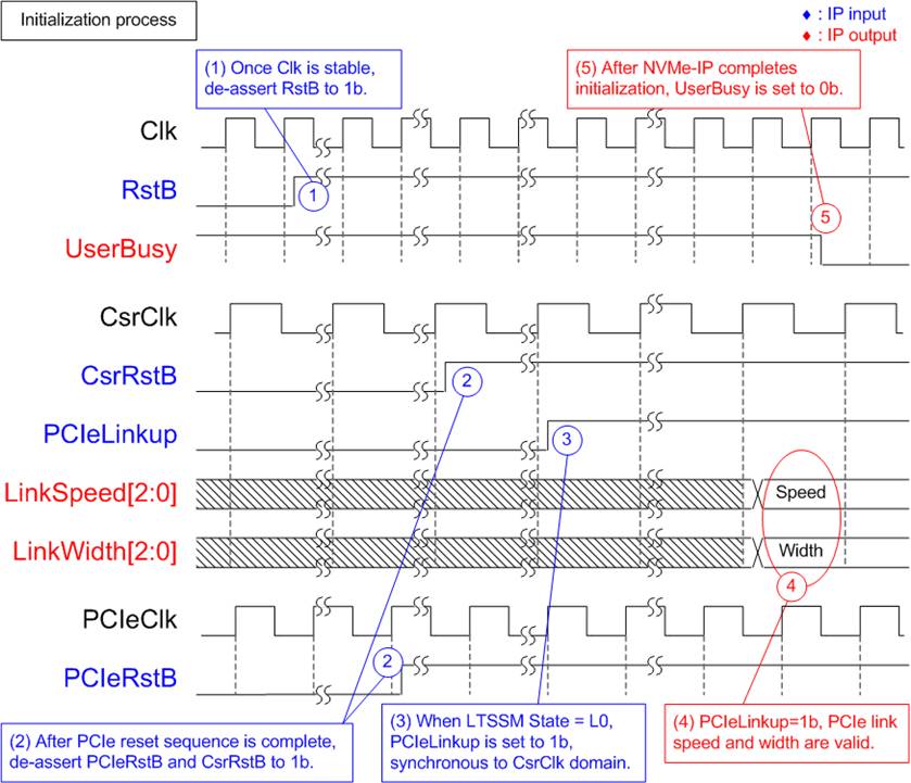
Figure 4 Timing Diagram During Initialization Process
The initialization process of the NVMe-IP follows the steps outlined below, as illustrated in the timing diagram:
1) De-assert RstB to 1b once the Clk signal is stable.
2) After the PCIe reset sequence is complete, de-assert both PCIeRstB and CsrRstB to 1b.
3) The PCIe Hard IP begins its initialization process and asserts PCIeLinkup to 1b once the LTSSM state reaches the L0 state. Since PCIeLinkup operates on CsrClk and is decoded from the LTSSM signal generated on PCIeClk, an asynchronous register must be used to properly synchronize the signal between clock domains.
4) Once PCIe initialization is complete, the user can read the PCIe link speed and link width from the NVMe-IP. These registers are synchronous with CsrClk, so the values must be converted to the user logic clock domain using asynchronous registers.
5) When the NVMe-IP completes its internal initialization, it de-asserts UserBusy to 0b, indicating that the IP is ready.
After all of the above steps are completed, the NVMe-IP is ready to receive user commands.
Control Interface of dgIF typeS
The dgIF typeS signals can be split into two groups: the Control interface for sending commands and monitoring status, and the Data interface for transferring data streams in both directions.
Figure 5 shows an example of how to send a new command to the IP via the Control interface of dgIF typeS.
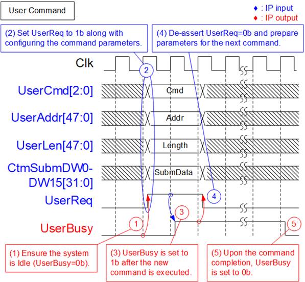
Figure 5 Control Interface of dgIF typeS Timing Diagram
1) UserBusy must be equal to 0b before sending a new command request to confirm that the IP is Idle.
2) Command and its parameters such as UserCmd, UserAddr, and UserLen must be valid when asserting UserReq to 1b to send the new command request.
3) IP asserts UserBusy to 1b after starting the new command operation.
4) After UserBusy is asserted to 1b, UserReq is de-asserted to 0b to finish the current request. New parameters for the next command could be prepared on the bus. UserReq for the new command must not be asserted to 1b until the current command operation is finished.
5) UserBusy is de-asserted to 0b after the command operation is completed. Next, new command request can be initiated by asserting UserReq to 1b.
Note: The number of parameters used in each command is different. More details are described below.
· Write and Read commands: UserCmd, UserAddr, and UserLen.
· SMART, Secure Erase, and Flush commands: UserCmd and CtmSubmDW0-DW15.
· Identify and Shutdown commands: UserCmd.
6)
Data Interface of dgIF typeS
Data interface of dgIF typeS is applied for transferring data stream when operating Write or Read command, and it is compatible with a general FIFO interface. Figure 6 shows the data interface of dgIF typeS when transferring Write data to the IP in the Write command.
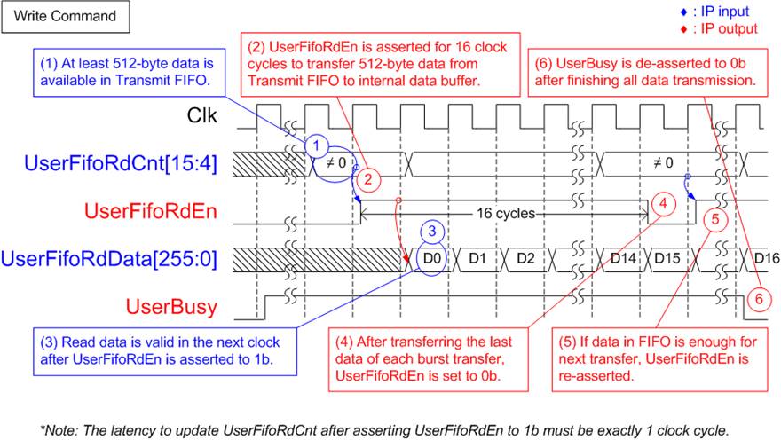
Figure 6 Transmit FIFO Interface for Write Command
The 16-bit FIFO read data counter (UserFifoRdCnt) indicates the total amount of data stored in the Transmit FIFO. When sufficient data is available, 512 bytes of data, equal to 16 × 256-bit words, are transferred.
For a Write command, data is read from the Transmit FIFO until the total transfer size has been completed. The data transfer process is described below.
1) Before starting a new burst transfer, the IP waits until at least 512 bytes of data are available in the Transmit FIFO. This condition is determined by monitoring UserFifoRdCnt[15:4], which must not be equal to zero.
2) The IP asserts UserFifoRdEn to 1b for 16 clock cycles to read 512-byte data from the Transmit FIFO.
3) UserFifoRdData becomes valid in the next clock cycle after asserting UserFifoRdEn to 1b, and 16 data words are transferred continuously.
4) After the 16th data word (D15) of each burst has been transferred, UserFifoRdEn is de-asserted to 0b.
5) Repeat steps (1) – (4) to transfer the next 512-byte block until the total amount of transferred data matches the transfer size specified in the command.
6) Once all data has been successfully transferred, UserBusy is de-asserted to 0b, indicating completion of the Write operation.
Note: For correct NVMe-IP operations, the latency between UserFifoRdCnt[15:0] and UserFifoRdEn must be exactly 1 clock cycle. If the system requires additional latency, please contact us for customized adapter logic.
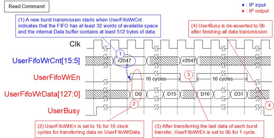
Figure 7 Receive FIFO Interface for Read Command
When executing the Read command, data is transferred from the SSD to the Receive FIFO until the entire data has been completely received. The burst data transfer process is described as follows:
1) Before starting a new burst transmission, UserFifoWrCnt[15:5] is checked to ensure that there is enough free space in the Receive FIFO, which is indicated by the condition UserFifoWrCnt[15:5] ≠ all 1s or 2047. The IP waits until there is enough free space available, and at least 512 bytes of data have been received from the SSD. Once both conditions are met, the new burst transmission begins.
2) The IP asserts UserFifoWrEn to 1b for 16 clock cycles to transfer 512-byte data from the Data buffer to the user logic.
3) After each 512-byte data transfer is completed, UserFifoWrEn is de-asserted to 0b for one clock cycle. If additional data remains to be transferred, repeat steps (1) – (3) until the total transferred data size matches the transfer size specified in the command.
IdenCtrl/IdenName
To ensure proper operation of the system, it is recommended to send the Identify command to the IP as the first command after the system boots up. This command updates important information about the SSD, such as its total capacity (LBASize) and LBA unit size (LBAMode), which are necessary for Write and Read commands to operate correctly. The following rules apply to the input parameters of these commands.
· The sum of the address (UserAddr) and transfer length (UserLen), inputs of Write and Read commands, must not exceed the total capacity (LBASize) of the SSD.
· If LBAMode is 1b (LBA unit size is 4 KB), the three lower bits (bits[2:0]) of UserAddr and UserLen must be set to 0 to align with the 4 KB unit.
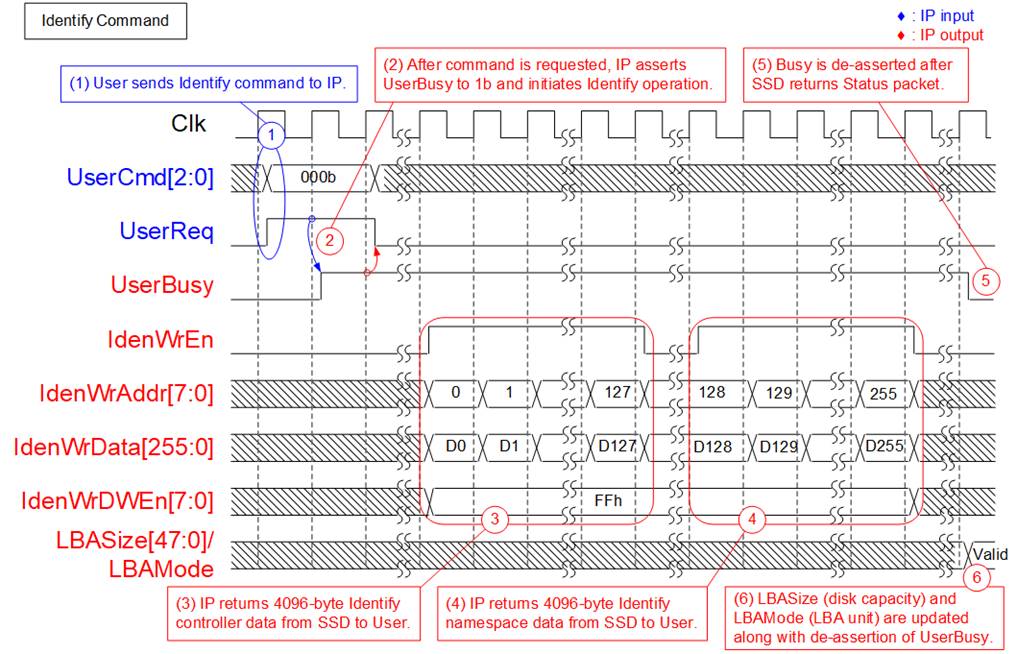
Figure 8 Identify Command Timing Diagram
When executing the Identify command, the following steps are taken.
1) Send the Identify command to the IP (UserCmd=000b and UserReq=1b).
2) The IP asserts UserBusy to 1b after receiving the Identify command.
3) The IP returns 4KB Identify controller data to the user with IdenWrAddr equal to 0-127 and asserts IdenWrEn. IdenWrData and IdenWrDWEn are valid at the same clock as IdenWrEn=1b.
4) The IP returns 4KB Identify namespace data to the user with IdenWrAddr equal to 128-255. IdenWrAddr[7] can be used to determine the data type as Identify controller data or Identify namespace data.
5) UserBusy is de-asserted to 0b upon the Identify command completion.
6) The LBASize and LBAMode of the SSD are simultaneously updated with the values obtained from the Identify command.
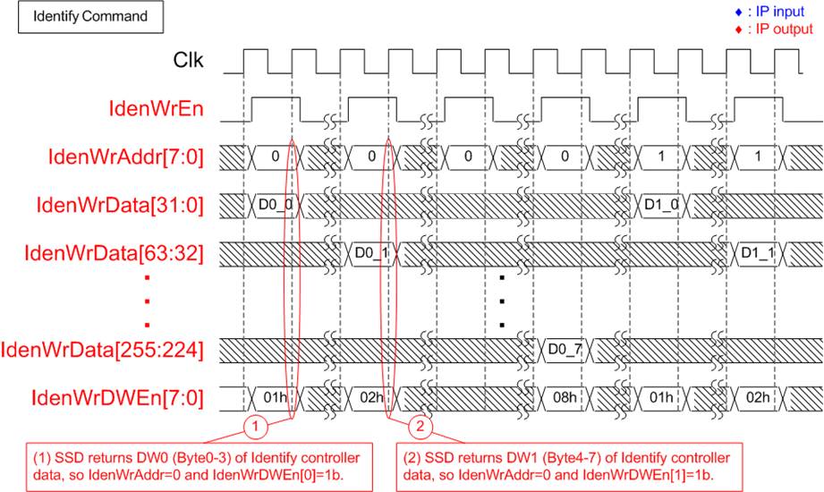
Figure 9 IdenWrDWEn Timing Diagram
The signal IdenWrDWEn is an 8-bit control signal used to validate corresponding segments of a 256-bit data bus that carries 32-bit words. This is used for SSDs that return 4KB Identify controller and Identify namespace data one 32-bit word at a time, rather than as a continuous stream.
To forward a single 32-bit word during a write cycle, one bit of IdenWrDWEn is asserted to 1b, as illustrated in Figure 9. Each bit of IdenWrDWEn corresponds to a specific 32-bit segment of IdenWrData: bit[0], [1], …, [7] of IdenWrDWEn map to bits[31:0], [63:32], …, [255:224] of IdenWrData, respectively.
Shutdown
The Shutdown command should be sent as the last command before the system is powered down. The SSD ensures that the data from its internal cache is written to the flash memory before the shutdown process finishes. After the shutdown operation is completed, the NVMe-IP and the SSD become inactive. If the SSD is powered down without executing the Shutdown command, the total count of unsafe shutdowns is increased, as indicated by data returned from the SMART command.
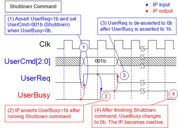
Figure 10 Shutdown Command Timing Diagram
The process for executing the Shutdown command is described below.
1) Ensure that the IP is in the Idle state (UserBusy=0b) before issuing the Shutdown command. To send the command request, the user must set UserReq=1b and UserCmd=001b.
2) Once the NVMe-IP starts executing the Shutdown command, UserBusy is asserted to 1b.
3) After UserBusy is asserted, UserReq is de-asserted to 0b to clear the current request.
4) When the SSD has completely shut down, UserBusy is de-asserted to 0b. After the shutdown process is complete, the IP no longer accepts any user commands.
SMART
The SMART command is the command to check the health of the SSD. When this command is sent, the SSD returns 512-byte health information. The SMART command parameters are loaded from the CtmSubmDW0-DW15 signals on the Custom command interface. The user must set the 16-Dword command data to fixed values before asserting UserReq. Once the SMART data is returned, it can be accessed via the Custom RAM I/F, as shown in Figure 11.
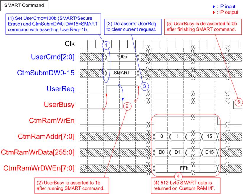
Figure 11 SMART Command Timing Diagram
Below are the details of how to execute the SMART command.
1) Ensure that the NVMe-IP is in the Idle state (UserBusy=0b) before issuing the command. All input parameters must maintain their values while UserReq is set to 1b to initiate the request. The CtmSubmDW0-DW15 fields must be set to fixed values for the SMART command as follows:
CtmSubmDW0 = 0000_0002h
CtmSubmDW1 = FFFF_FFFFh
CtmSubmDW2 – CtmSubmDW5 = 0000_0000h
CtmSubmDW6 = 2000_0000h
CtmSubmDW7 – CtmSubmDW9 = 0000_0000h
CtmSubmDW10 = 007F_0002h
CtmSubmDW11 – CtmSubmDW15 = 0000_0000h
2) Once the command is accepted, the IP asserts UserBusy to 1b, indicating that the command is being executed.
3) After the request has been acknowledged, de-assert UserReq to 0b to clear the current command. Next, the user logic may update the input parameters for the next command.
4) The 512-byte SMART data is returned on the CtmRamWrData signal, with CtmRamWrEn set to 1b. CtmRamAddr ranges from 0 to 15, representing the index of each 32-byte segment within the 512-byte block. When CtmRamAddr=0, bytes 0-15 of SMART data are valid on CtmRamWrData. CtmRamWrDWEn indicates the validity of each 32-bit CtmRamWrData. If CtmRamWrDWEn=FFh, CtmRamWrData[255:0] are valid.
5)
When the SMART command has
completed, UserBusy is de-asserted to 0b.
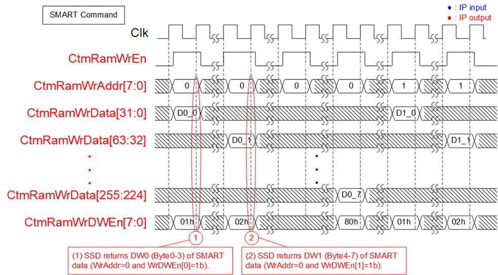
Figure 12 CtmRamWrDWEn Timing Diagram
Similar to Identify command, some SSDs return only one Dword (32-bit) of data at a time instead of streaming 512-byte block continuously. In such cases, one bit of CtmRamWrDWEn is asserted to 1b during the write cycle to indicate that a specific 32-bit segment of CtmRamWrData is valid. Each bit of CtmRamWrDWEn corresponds to a 32-bit segment within the 256-bit CtmRamWrData signal as follows: bit[0], [1], [2], …, and [7] of CtmRamWrDWEn correspond to bits[31:0], [63:32], …, and [255:224] of CtmRamWrData, respectively.
Secure Erase
The Secure Erase is a command that erases all user data in the SSD. After the Secure Erase command is executed, the contents of the user data are indeterminate. Since executing this command may require long time for operation, users need to disable the IP timer by setting ‘TimeoutSet’ signal to zero.
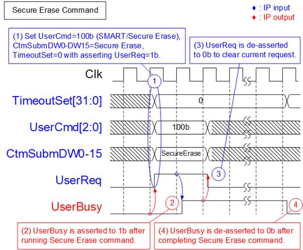
Figure 13 Secure Erase Command Timing Diagram
Below are the details of how to execute the Secure Erase command.
1) Ensure that the NVMe-IP is in the Idle state (UserBusy=0b) before issuing the command. All input parameters must maintain their values while UserReq is set to 1b to send the request. The TimeoutSet and CtmSubmDW0-DW15 fields must be set to fixed values for the Secure Erase command as follows:
TimeoutSet = 0000_0000h (Disable Timer)
CtmSubmDW0 = 0000_0080h
CtmSubmDW1 = 0000_0001h
CtmSubmDW2 – CtmSubmDW9 = 0000_0000h
CtmSubmDW10 = 0000_0200h
CtmSubmDW11– CtmSubmDW15 = 0000_0000h
2) Once the command is accepted, the IP asserts UserBusy to 1b, indicating that the command is being executed.
3) After the request has been acknowledged, de-assert UserReq to 0b to clear the current command. Next, the user logic may update the input parameters for the next command.
4) When the Secure Erase command has completed, UserBusy is de-asserted to 0b. Following this, the ‘TimeoutSet’ can be changed to other values to enable timeout function of the IP.
Note: Some SSDs may experience a decrease in performance after long data transfer. In such cases, executing the Secure Erase command can help restore the SSD’s performance
Flush
The SSDs typically enhance write performance by caching write data before writing it to the flash memory. However, unexpected power loss can result in data loss as cached data may not be stored in flash memory. To avoid data loss, the Flush command can be used to force the SSD controller to write cached data to the flash memory.
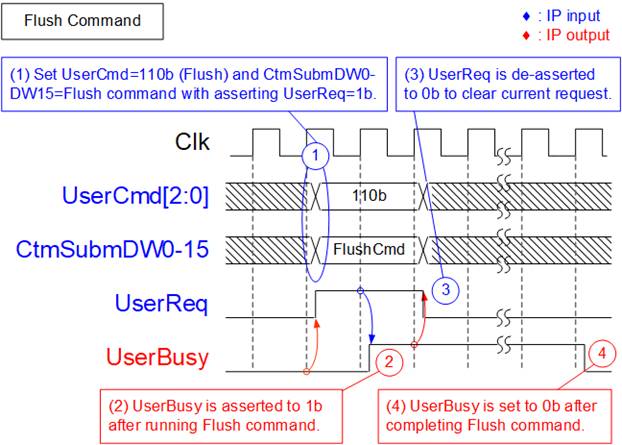
Figure 14 Flush Command Timing Diagram
To execute the Flush command, follows the steps outlined below:
1) Ensure the IP is the Idle state (UserBusy=0b) before sending the command request. All input parameters must maintain their values while UserReq is set to 1b for sending the request. For the Flush command, the CtmSubmDW0-DW15 fields must be set to fixed values as follows:
CtmSubmDW0 = 0000_0000h
CtmSubmDW1 = 0000_0001h
CtmSubmDW2 – CtmSubmDW15 = 0000_0000h
2) Once the command is accepted, the IP asserts UserBusy to 1b, indicating that the command is being executed.
3) After the request has been acknowledged, de-assert UserReq to 0b to clear the current command. Next, the user logic may update the input parameters for the next command.
4) When the Flush command has completed, UserBusy is de-asserted to 0b.
Using the Flush command ensures that all data from the previous Write operations is guaranteed to be stored in flash memory, thus preventing data loss in the event of unexpected power loss.
Error
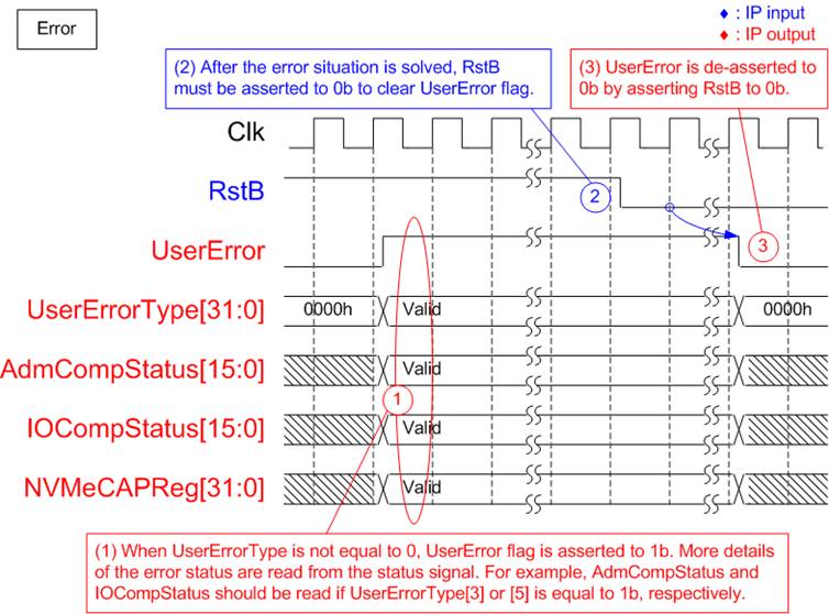
Figure 15 Error Flag Timing Diagram
If an error occurs during the initialization process or while executing a command, the UserError flag is set to 1b. To identify the type of error, the UserErrorType signal should be examined. Additionally, the NVMeCAPReg, AdmCompStatus, and IOCompStatus signals can be used to monitor error details after UserError is asserted.
If the error occurs during initialization, it is recommended to read the NVMeCAPReg signal to verify the capabilities of the connected NVMe SSD. If the error occurs during command execution, it is recommended to check the AdmCompStatus and IOCompStatus signals.
· If bit[3] of UserErrorType is asserted, refer to the AdmCompStatus signal for more detailed error information.
· If bit[5] of UserErrorType is asserted, refer to the IOCompStatus signal for further details.
The UserError flag is cleared only by asserting the RstB signal. Once the issue is resolved, assert RstB to 0b to reset the IP and clear the error status.
Verification Methods
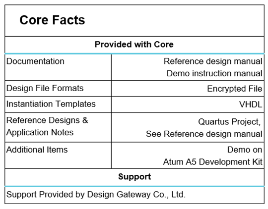
The NVMe IP Core for Gen4 functionality was verified by simulation and also proved on real board design by using Atum A5 development kit.
Recommended Design Experience
Experienced design engineers with knowledge of Quartus tools should easily integrate this IP into their design.
Ordering Information
This product is available directly from Design Gateway Co., Ltd. For pricing and additional information about this product, please refer to the contact information on the front page of this datasheet.
Revision History
|
Revision |
Date (D-M-Y) |
Description |
|
1.00 |
8-Jul-26 |
Initial release |