Unboxing the #1 FPGA Based NVMe IP core from Design Gateway
In the era of AI, real-time data processing, and edge computing, high-speed storage access is no longer optional—it’s essential. That’s why we’re excited to introduce the NVMe-IP core from Design Gateway—a solution engineered for FPGA platforms that demand performance, reliability, and simplicity.
🎥 Watch the Unboxing Video on YouTube
⚡ What Makes NVMe-IP Core #1?
The NVMe-IP Core is more than just an IP block—it’s a ready-to-integrate FPGA storage solution that eliminates the need for NVMe protocol expertise. It’s designed for engineers who want to skip months of integration effort and go straight to performance.
- Plug-and-play reference design
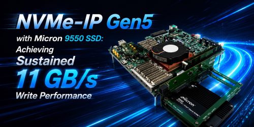
- Write speeds up to 3100 MB/s (Agilex 5 demo)
- Supports Altera & AMD/Xilinx FPGAs
- No CPU, no external DDR memory needed
- 7 built-in commands including Write, Read, SMART, Secure Erase, and Flush
🔍 Why NVMe-IP from Design Gateway?
- No NVMe Protocol Knowledge Required The IP comes with an out-of-the-box reference design, so you can integrate it without spending time learning the NVMe protocol stack.
- Performance that Speaks Volumes Tested on the latest Sulfur Agilex 5 FPGA, our demo achieves 3100 MB/s write speed, outperforming previous platforms by a significant margin.
- Professional Documentation From VHDL module breakdowns and firmware explanations to real signal timing diagrams—you’ll have everything you need to develop, customize, and deploy with confidence.
- Broad Hardware Support Compatible with major Altera FPGAs like Agilex, Arria, Stratix, and Cyclone series, and tested with AB18, AB19, and AB20 PCIe adapter boards.
- Free Evaluation Available Yes—you can try the IP for free! Download the SOF file and test it on your own FPGA board before you buy.
📦 What’s Inside the NVMe-IP Package?
The IP core package includes:
✅ Pre-built Quartus/Vivado projects
✅ HDL modules with detailed documentation
✅ Embedded firmware with full source code
✅ SOF files for fast prototyping
✅ Evaluation-ready setup—test before you buy!
Whether you’re working on defense-grade systems, high-speed imaging, AI inference, or financial trading platforms, NVMe-IP ensures deterministic latency and real-time throughput.
🧪 See It in Action
In our latest demo, we tested the NVMe-IP on the Altera Sulfur Agilex 5 FPGA using the AB19 M.2-PCIe adapter board and achieved a blazing 3100 MB/s write speed—a noticeable boost over previous generations.
🔗 Download the Evaluation SOF file for Free: https://dgway.com/download/download_form.html?d=NVMeIPTest_Config_SulfurAG5.zip
📌 Perfect for:
✅ FPGA Engineers
✅ Embedded Developers
✅ Industrial System Designers
✅ AI & Robotics Innovators
✅ Data Acquisition Experts
✅ Research Institutions
📬 Ready to explore?
📥 Contact our team at https://dgway.com/contact.html
🌐 Visit the product page: https://dgway.com/NVMe-IP_A_E.html
🛠️ Want to try it yourself? Download the free SOF file, test it on your FPGA, and experience true high-performance NVMe storage.
If you’re passionate about next-generation FPGA storage, low-latency systems, or building high-performance hardware, follow us for more IP releases, demos, and customer stories.
🔁 Like, 💬 Comment, and 🔗 Share this with your team or anyone exploring NVMe solutions on FPGA.