High performance AES256-GCM for secure communication over 100G Ethernet
Secure communication with cryptographic algorithms needs a lot of computation power. Especially, In the Data Center with very high bandwidth networking such as 25G, 100G or more!.
Trusted protocols such as TLS and SSL can be processed in real-time at 100Gbps with Hardware Acceleration. AES-GCM is recommended symmetric-key cryptographic block ciphers for TLS and SSL, approved by NIST.
Design Gateway’s AES256-GCM IP Core is designed to meet NIST standards with high performance throughput over 100Gbps. It’s suitable TLS and SSL offload and acceleration by FPGA for any application that required 100G throughput over secure network communication.
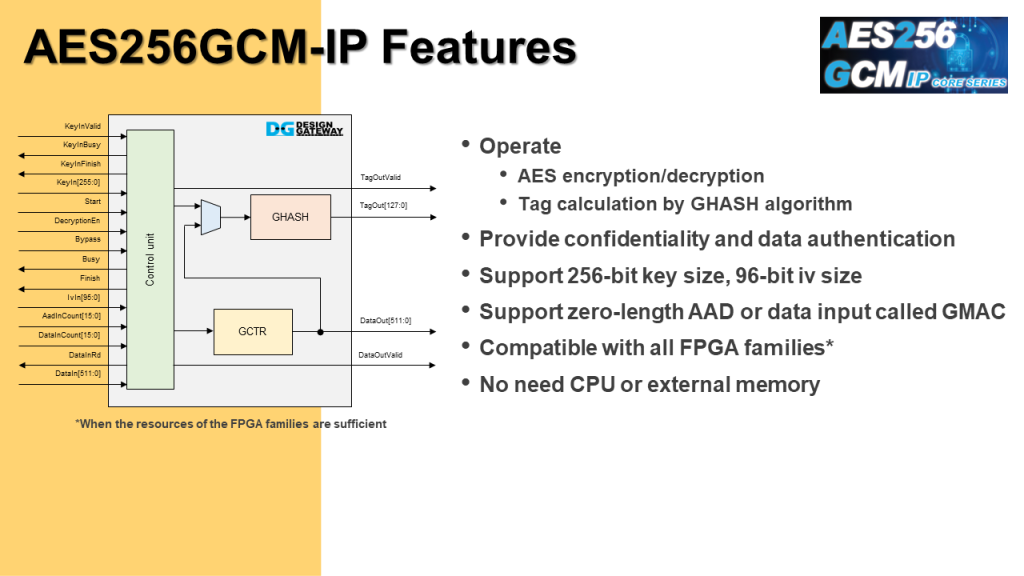
AES256 GCM IP Core implement the advanced encryption standard in Galois Counter Mode.
There are 2 main operations in AES GCM, AES encryption/decryption and tag calculation by GHASH algorithm.
Key features
- Provide confidentiality and data authentication by using Additional Authenticated Data (AAD) and authentication tag.
- Supports 256 bit AES key and 96 bit Initialization Vector.
- Support zero length AAD or zero length data input called GMAC.
- Compatibility with all FPGA families.
- No need CPU or external memory.
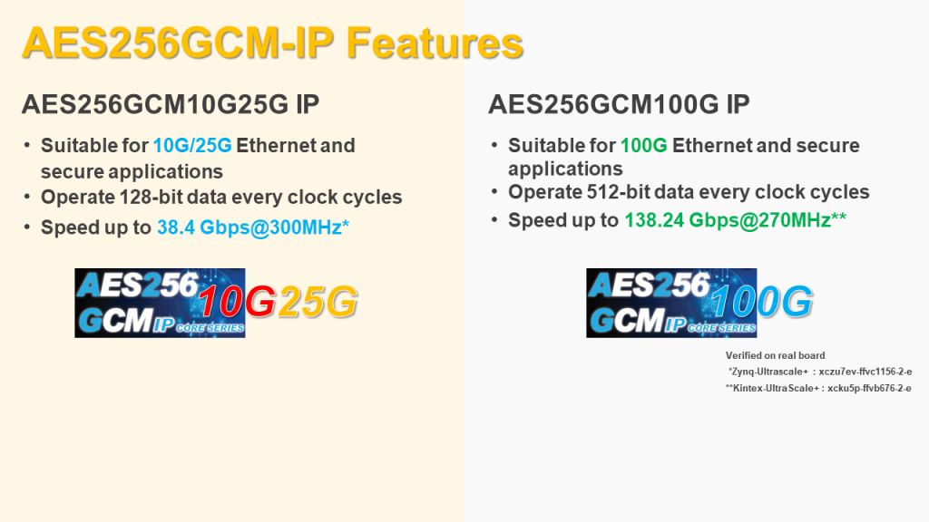
There are two products of AES256 GCM IP.
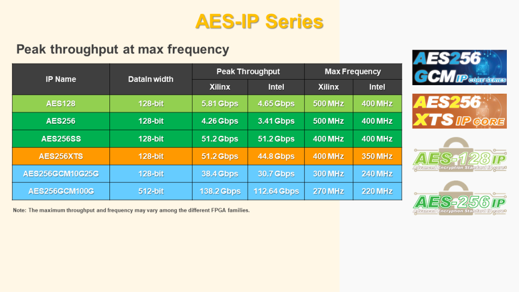
First, AES256 GCM 10G/25G.
- Suitable for 10G/25G Ethernet.
- Operate 128-bit data every clock cycle.
- High-throughput, up to 38.4 Gbps @300MHz.
Second, AES256 GCM 100G.
- Suitable for 100G Ethernet.
- Operate 512-bit data every clock cycle.
- High-throughput, up to 138.24 Gbps @270MHz.
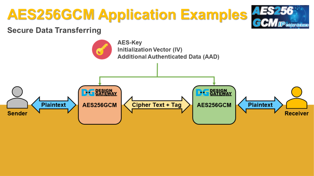
AES256 GCM IP can be used for secure data storage application or secure communication over a computer network.
Before transferring data, sender encrypt data with AES key, AAD and IV, which these three AES-GCM parameters are known only sender and receiver.
Receiver use the same AES GCM parameters to decrypt data and use authentication tag to check whether transferred data is modified.
If tag which is attached with encrypted data is matched with tag generated by receiver, it confirms that received data came from the sender and the encrypted data is not changed.
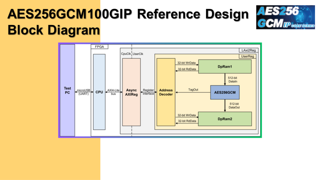
Here is the block diagram of AES256 GCM demo reference design.
In the test environment, AES256 GCM IP interface with two dual-port RAMs with asymmetric ports.
CPU system is designed to interface with FPGA logict hrough AXI4 Lite bus and interface with user through serial console in test PC.
Let’s see the demonstration on Xilinx ZCU106 Evaluation board
We provide AES256-GCM IP functional demonstration on Xilinx ZCU106 Evaluation Board.
In the demonstration, AES256-GCM IPs are used to encrypt and decrypt data between two memories in FPGA and provide an authentication tag.
Users can fill memory with Additional Authenticated Data (AAD), plain or cipher data patterns, set encryption/decryption key, Initialization Vector (IV), and control test operation via serial console.
- Set encryption key and decryption key, press enter 0.
- Set initialization vector for encryption and decryption, press enter 1.
- Clear plain data memory by fill all zero, press enter 2.
- Fill AAD memory by fill 8-bit counter, press enter 3 and b.
- Fill data memory by fill 16-bit counter, press enter 4 and c.
- Encrypt data, press enter 5.

After encryption is done, AAD input, Data input, AAD output, Data output and Tag are displayed.
- Decrypt data, press enter 6.
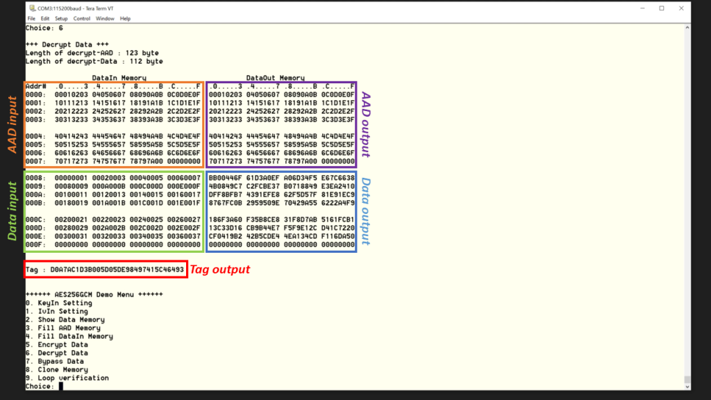
Input and output for decryption are displayed.
- Verification data, press enter 9.
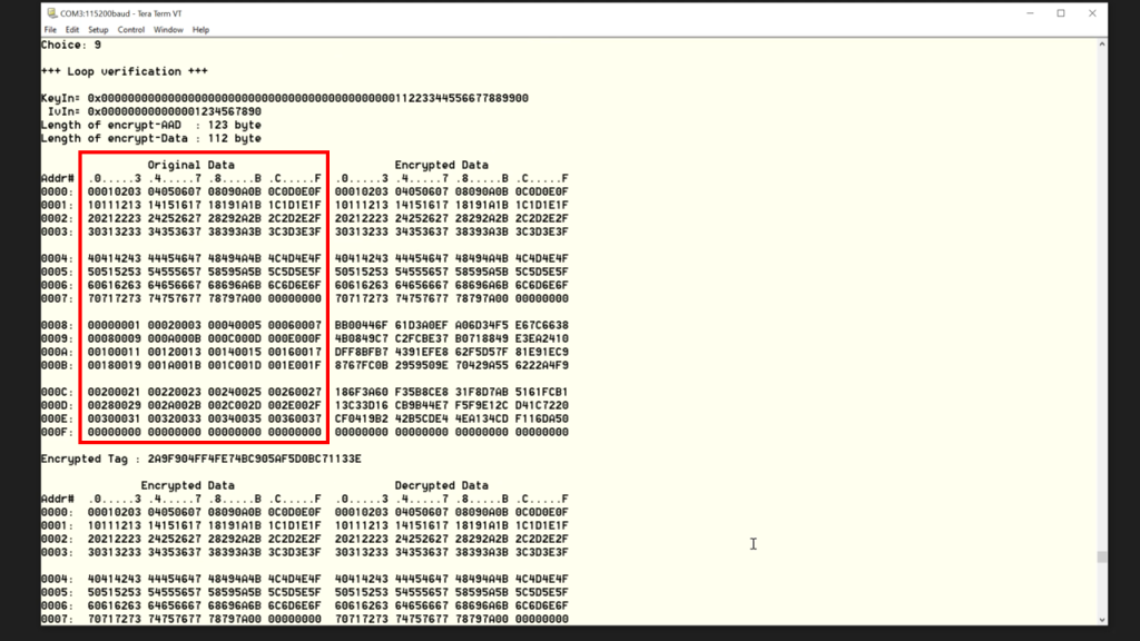
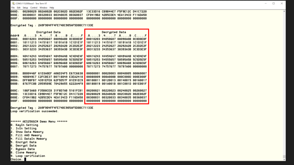
After loop verification, the user can observe that the original data corresponds to the decrypted data.
In addition to AES-GCM, explore the other available mode of operations displayed in the table above.
For more information Please visit our website: https://dgway.com/index_E.html
Youtube: https://youtu.be/sM2s4z8gioM