Achieving 11,463 MB/s NVMe Gen5 Performance with AES-XTS on Altera Agilex 7 FPGA
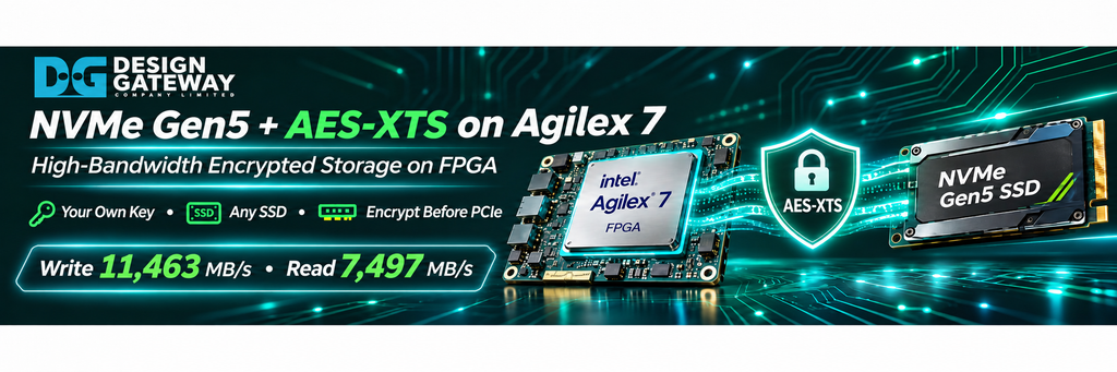
Design Gateway introduces high-bandwidth NVMe Gen5 storage with AES-XTS encryption on Altera Agilex 7 FPGA — using your own key, on any SSD.
As storage bandwidth scales up with Gen5 SSDs, protecting sensitive data with your own key inside the FPGA—rather than relying on drive-level encryption—becomes essential. This walkthrough covers how AES-XTS IP and NVMe Gen5 IP operate together on an Agilex 7 FPGA board connected to an enterprise Gen5 SSD, along with sustained write and read benchmark results.
Watch the Full Demonstration
See the full demo: Altera Agilex 7 FPGA NVMe Gen5 Demo | AES-XTS Encryption at 11,463 MB/s
Core Architecture Highlights
AES-XTS IP and NVMe Gen5 IP run together inside the Altera Agilex 7 FPGA so data is encrypted before it leaves the chip with your own key.
Full Gen5 Bandwidth
Inline AES-XTS encryption inside Agilex 7 FPGA
Your Own Key
Key loaded into FPGA before data leaves chip
Any SSD
Works across SSDs without trusting SED black box
Encrypting Before Data Leaves the FPGA
Gen5 SSDs can record data at many gigabytes per second. When handling Gen5 data streams—such as data moving from a sensor or camera through an FPGA NVMe host at 11,000 MB/sec—a key question arises: who holds the key, and how do you protect that data across the PCIe link?
Rather than relying on encryption tucked inside the drive itself, running cryptographic processing directly inside the FPGA ensures data is protected before it leaves the chip—using your own key, on any SSD.
Black-Box Drive
Self-Encrypting Drives (SED)
An NVMe SSD self-encrypting drive (Opal) keeps SED firmware and the encryption key inside the drive—a black box you have to trust.
Data still travels across the PCIe link as plain text before reaching the drive’s internal encryption.
Agilex 7 FPGA IP
Design Gateway FPGA IP Solution
With Design Gateway IP, AES-XTS IP and NVMe Gen5 IP run together inside the Altera Agilex 7 FPGA so data is encrypted before it leaves the chip.
Encryption uses your own key loaded into the FPGA, enabling full Gen5 bandwidth protection across any SSD.
Key Control
Key stays inside the SSD
You cannot load or control it yourself.
Firmware Trust
Closed, unauditable firmware
Security rests on trusting the drive vendor.
PCIe Link Risk
Plaintext on the PCIe link
Data travels across the PCIe link unencrypted before reaching drive encryption.
Sustained Read & Write Performance
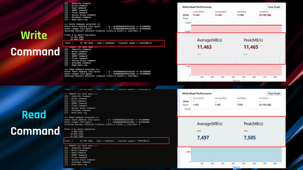
Tested on an Agilex 7 FPGA board connected to an enterprise Gen5 SSD in a 25.77 GB sequential transfer test.
11,463 MB/s
Sustained Write Speed (Full Transfer)
7,497 MB/s
Sustained Read Speed (Same SSD Capacity)
Demo Setup & Test Execution
For this setup, we’re using the Agilex 7 FPGA board connected to an enterprise Gen5 SSD. Once we power on the board and load the demo file, we have a menu ready for testing.
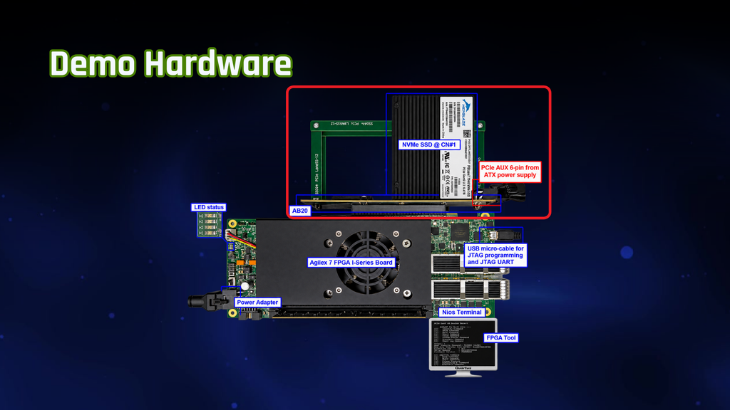
Hardware Setup: Agilex 7 FPGA I-Series Board, NVMe SSD @ CN#1, PCIe AUX 6-pin power, USB JTAG/UART cable, and Nios Terminal test menu.
1
Power On & Load Demo File
Connect the Agilex 7 FPGA board to an enterprise Gen5 SSD, power on the board, and load the demo file so the test menu is ready.
2
Run Full Write Transfer
Run a full transfer across the drive to observe a sustained write speed of 11,463 megabytes per second.
3
Run Full Read Command
Execute the read command across the same SSD capacity to observe a sustained read speed of 7,497 megabytes per second.
High Bandwidth, Uncompromised Security
Both sustained speeds are achieved while data is fully protected by AES-XTS encryption—with no CPU and no external memory required.
No CPU Required
No External Memory Required
Full AES-XTS Protection
Final Key Takeaway
Design Gateway's NVMe Gen5 IP and AES-XTS IP enable direct, hardware-accelerated encrypted storage on Altera Agilex™ 7 FPGA logic—protecting data with your own key before it ever leaves the chip. Delivering sustained write speeds up to 11,463 MB/s and read speeds up to 7,497 MB/s with no CPU and no external memory required, this architecture provides deterministic Gen5 performance and uncompromising data security across any enterprise NVMe SSD.
Agilex 7 IP Solution & Resources
Maximum Gen5 Performance & Ultimate Data Security for Agilex 7
With Design Gateway’s IP, you get maximum Gen5 performance and ultimate data security for your Agilex 7 designs.
Contact us to find the right secure NVMe solution for your FPGA system, or explore the datasheets, reference designs, and evaluation demos below to learn more.
NVMe Gen5 IP
High-Speed Storage Host
NVMe Gen5 Datasheet
→
NVMe Gen5 Reference Design
→
Free Demo (Agilex 7 I-Series)
ZIP
AES256-XTS IP
Hardware Data Encryption
AES256-XTS IP Datasheet
→
AES256-XTS Reference Design
→
Free Demo (Agilex 7 I-Series)
ZIP
Need help choosing the right secure NVMe architecture?
Our FPGA specialists are ready to assist with your Agilex 7 design.