#002 Using Multiple DDR Banks
Based on Xilinx’s VitisTM Application Acceleration Development Flow Tutorial:
By default, the data transfer between the Kernel and the DDR is accomplished by using single DDR. In some applications, transferring large amount of data between global memory (DDR) and FPGA can be a cause of performance dropped. Using multiple DDR banks can be one of the solutions. Therefore, this tutorial illustrates you how to map kernel ports to multiple DDR banks.
Overviews
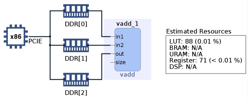
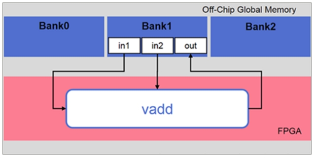
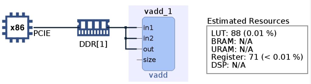
In this tutorial, it uses a simple vector addition, called ‘vadd’. The ‘vadd’ kernel is reading data from ‘in1’ and ‘in2’ and the result is ‘out’. The basic behavior of Vitis core development is to use only a single DDR bank to exchange data between kernel and global memory. In this case, all the data access of port ‘in1’, ‘in2’ and ‘out’ of ‘vadd’ kernel come from the default DDR bank only, as shown in picture below.
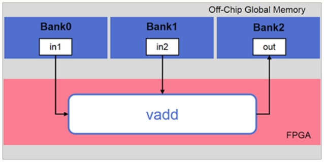
The picture below demonstrates a plan to reduce the load of access data by using multiple DDR which will carry out in this tutorial later.
Step by step to run on TKAS
Using set environment and old folder from last issue. Then, navigate to ./Hardware_Acceleration/Feature_Tutorials/04-mult-ddr-banks/reference-files
Changing configuration for Alveo U250 card
File makefile
Line 4 | PLATFORM := xilinx_u250_gen3x16_xdma_3_1_202020_1
Save makefile and close.
Build & Check
Execute the command below in order to see the default behavior of Vitis core development tool
make all
After execute command, user would see the console indicate the default behavior as picture below
To ensure the automatically mapping of Vitis development core, user can be used option ‘check’ when execute ‘make’ command as below.
make check
After the simulation complete, the report of memory transfer is generated as shown below.
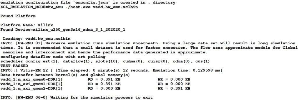
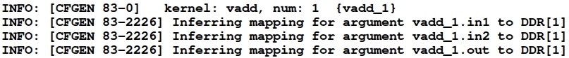
As you can see, all data transfer is done by using DDR bank 1 only. User can view it as graphic by using command below
vitis_analyzer vadd.hw_emu.xclbin
From now on, this is steps to use multiple DDR in order to reduce bottleneck due to using single DDR data transfer.
Set v++ Linker options
navigate to ./Hardware_Acceleration/Feature_Tutorials/04-mult-ddr-banks/reference-files
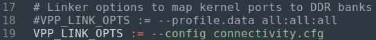
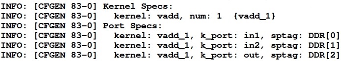
Open the makefile comment line 18 and uncomment line 19 in order to use file connectivity.cfg instead of using default behavior of Vitis development core relevant to mapping DDR bank, as shown in picture below.
The connectivity.cfg file is shown below.
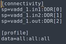
sp = <kernel_cu_name>.<kernel_arg>:<sptag>
sp : the option to allow user to map kernel port to a specific global memory banks.
<kernel_cu_name> : The compute unit (CU) based on the kernel name followed by ‘_’ and index.
<kernel_arg> : The function argument of the CU, for this tutorial is argument as found in ‘vadd.cpp’ file
<sptag> : Represents a memory resource available on the target platform.
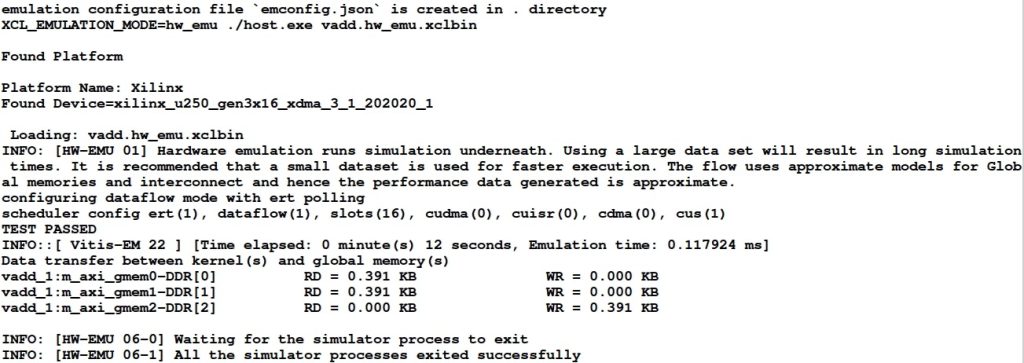
Build & Check
Execute the command below in order to perform multiple DDR banks
make all
After execute command, user would see the console indicate the default behavior as picture below
To confirm using multiple DDR by using makefile with option check as shown below
make check
After test is completed, the message shows as below
Furthermore, to view a graphic of multiple DDR bank by using below command
vitis_analyzer vadd.hw_emu.xclbin