Case Study: Validating NVMe SSD Sustained Throughput and Buffer Needs for Continuous Data Logging

Case Study Overview: In mission-critical edge recording and continuous instrumentation, relying on peak SSD datasheets often results in catastrophic data loss. This case study demonstrates how empirical testing on the AMD Kintex™ UltraScale™ FPGA KCU105 Evaluation Kit using Design Gateway’s NVMe™ SSD Characteristic Test Platform validates sustained read/write throughput and precisely identifies external DDR buffer requirements.
Modern high-speed data acquisition systems—ranging from radar sensing to multi-camera vision platforms—require consistent, deterministic storage throughput. However, system architects frequently encounter unexpected bandwidth drops during continuous operations. Understanding drive characteristics under long-duration workloads is the key to achieving robust system integration without expensive over-provisioning.
Real-World Impact: Where Zero Data Loss is Mandatory
In non-critical consumer devices, temporary write latency spikes are easily masked by OS-level memory caching. However, mission-critical edge instrumentation cannot tolerate even microsecond-level storage stalls:
Autonomous Vehicles & ADAS
Simultaneous ingestion from multiple 4K raw HDR camera sensors, LiDAR arrays, and radar streams requires sustained continuous logging rates of multiple GB/s without a single dropped frame during on-road safety validation.
Defense & Aerospace RF Capture
Direct RF signal digitizing and high-speed spectrum logging demand uninterrupted sequential writes. Any SSD buffer overflow results in corrupted telemetry or unrecoverable radar waveforms.
100G/400G Network Packet Capture
Line-rate network traffic monitoring and deep packet inspection (DPI) platforms mandate predictable write endurance and zero dropped packets across continuous multi-terabyte recording sessions.
The Challenge: Sustained Write Collapse
Not all NVMe™ SSDs behave equally under continuous, long-term write pressure. While datasheets boast multi-gigabyte speeds, those metrics typically measure short-burst operations.
Consumer SSDs (Burst-Optimized)
Rely heavily on internal SLC cache regions to boost short-term benchmark performance. Once the cache buffer is saturated, throughput plummets dramatically and fluctuates unpredictably, making them prone to FIFO overflows in real-time streaming.
Enterprise SSDs (Sustained Workloads)
Engineered with heavy over-provisioning and advanced wear-leveling algorithms to maintain steady sequential write performance over hours of continuous recording, guaranteeing deterministic Quality of Service (QoS).
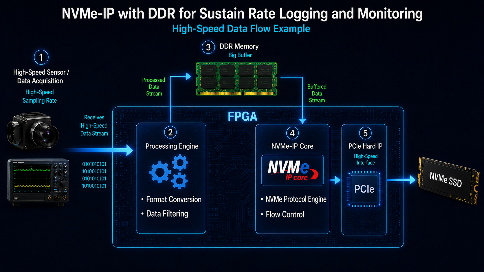
Figure 1: High-Speed Continuous Data Logging Architecture using Design Gateway NVMe-IP Core and DDR Memory Buffer.
The Solution: NVMe SSD Characteristic Test Platform
To eliminate performance guesswork before PCB fabrication, Design Gateway developed an FPGA-centric evaluation platform running entirely in pure hardware logic (no embedded OS, CPU, or software driver bottlenecks).
1. Parametric Speed Setting
Users configure precise target write/read throughput rates to systematically stress-test the drive under realistic streaming bandwidth demands.
2. Configurable DDR Buffer
Allows engineers to dynamically vary intermediate memory buffer sizes to determine how much reserve capacity is required to smooth out drive latency spikes.
3. Pass / Fail Validation
Delivers an immediate Pass/Fail status indicating whether the drive maintained uninterrupted throughput without triggering a buffer overflow condition.
Empirical Results: Identifying the Critical Buffer Threshold
The platform was evaluated on the AMD Kintex™ UltraScale™ FPGA KCU105 Evaluation Kit equipped with a Design Gateway AB18-PCIe®X16 adapter and an Intel® Optane™ SSD 900P. A continuous 280 GB LFSR payload was streamed across varying target speeds.
Experimental Methodology & Hardware Setup
To establish a reliable performance baseline, the evaluation benchmarked continuous sequential writing without host CPU intervention:
FPGA Target Platform
AMD Kintex™ UltraScale™ FPGA KCU105 Evaluation Kit utilizing pure RTL logic (Design Gateway NVMe™-IP core with external DDR4 memory buffer).
Storage Interface
Design Gateway AB18-PCIe®X16 adapter board directly hosting an Intel® Optane™ SSD 900P via PCIe® Gen3 x4 interface.
Why Intel® Optane™
3D XPoint architecture provides exceptionally flat write latencies without SLC-cache depletion, measuring pure FPGA-to-SSD throughput limits rather than drive throttling.
Stress Workload
Continuous 280 GB pseudo-random LFSR stream tested across stepped bandwidth targets (1,000 to 2,800 MB/s) with real-time peak DDR buffer monitoring.
2,800 MB/s
Max Sustained Write Verified
1,500 – 2,285
Critical Speed Threshold (MB/s)
0% CPU / OS
Pure Hardware FPGA Implementation
Key Architecture Insight: Internal FIFO vs. External DDR
The test data revealed an abrupt behavioral shift: below 1,500 MB/s, maximum buffer utilization stayed within standard kilobyte ranges, indicating that an internal FPGA Block RAM / UltraRAM FIFO is fully sufficient. However, crossing beyond 2,285 MB/s caused peak buffer demand to scale sharply into hundreds of megabytes. At these high data rates, incorporating external DDR memory becomes mandatory to absorb extended SSD write-cycle latencies.
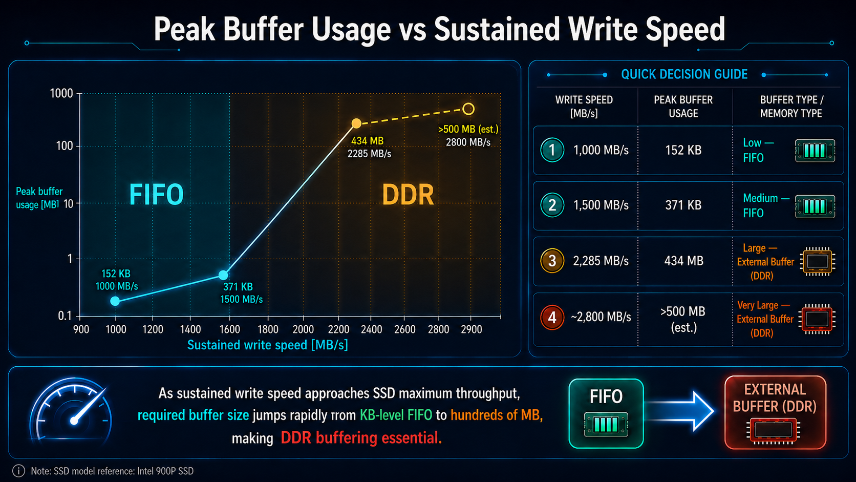
Figure 3: Measured Peak Buffer Usage scaling sharply between 1,500 MB/s and 2,285 MB/s.
Conclusion: System Right-Sizing & Verification
As demonstrated in this case study, continuous sustained-rate recording cannot rely solely on headline SSD specs. Empirical testing on the AMD Kintex™ UltraScale™ FPGA KCU105 clearly reveals drive latency characteristics and identifies the exact threshold where external DDR becomes mandatory. Sizing memory buffers based on actual benchmark data prevents costly hardware re-spins, ensures zero data loss, and eliminates over-engineering.
Case Study Verification Resources
Live Demonstration: Sustained Rate & Buffer Verification
Watch the NVMe™ SSD Characteristic Test Platform in action on the AMD Kintex™ UltraScale™ FPGA KCU105 board, demonstrating real-time throughput tracking, pass/fail evaluation, and dynamic DDR buffer usage measurement:
DEMO VIDEO

NVMe-IP DDR Reference Design
Sustained Data Rate Demo on AMD Kintex™ UltraScale™ FPGA KCU105
Replicate on Real Hardware: Free Evaluation Bitfile
Engineers can independently replicate the tests from this case study or profile their own target NVMe™ SSD drives on the AMD Kintex™ UltraScale™ FPGA KCU105 board. Select the package that matches your adapter hardware setup:
Ready to Validate Your Sustained Data Logging Solution?
Design Gateway provides complete reference designs, IP cores, and engineering support for high-throughput storage applications on AMD Kintex™ UltraScale™ platforms.