Accelerate NVMe Storage to 7,400 MB/s on Altera Agilex™ 5 FPGA without CPU and External Memory
High-speed edge data logging, radar signal processing, and autonomous vehicle telemetry demand sustained, multi-gigabyte-per-second storage throughput. Traditional CPU-based storage stacks can introduce OS kernel overhead, unpredictable latency, and additional power consumption. Design Gateway’s NVMe-IP addresses this bottleneck with a 100% hardware-offloaded PCIe Gen4 storage engine for the Altera Agilex™ 5 FPGA, achieving sustained transfer speeds above 7,400 MB/s without CPU intervention or external DDR memory.
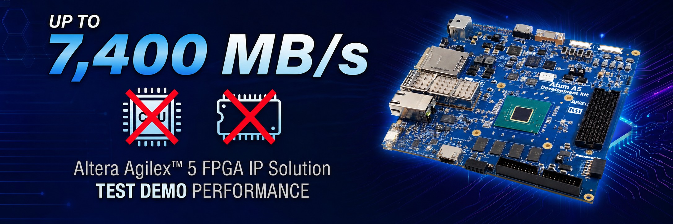
🎥 Watch the Full Demonstration
See the full demo NVMe IP on Altera Agilex 5 FPGA
⚙ The Edge Bottleneck and the Agilex™ 5 Advantage
As system architectures move closer to the edge, engineers face a dual challenge: maximizing throughput while limiting power consumption, form factor, and board complexity. The Altera Agilex™ FPGA portfolio addresses a range of operational requirements across three main tiers:
- Agilex™ 3: Optimized for power- and cost-sensitive edge applications.
- Agilex™ 5: Designed for embedded and edge applications, combining advanced DSP and AI Tensor blocks with PCIe Gen4 hard IP.
- Agilex™ 7 and Agilex™ 9: Designed for high-end compute, cloud, and direct RF applications.
By using the Altera Agilex™ 5 FPGA, Design Gateway’s NVMe-IP enables deterministic, High-Throughput NVMe SSD access directly from FPGA logic. The IP core interfaces with an enterprise-class PCIe Gen4 U.2 SSD without requiring an embedded processor such as Arm or Nios, or an external DDR buffer.
⚙ Architecture Highlights: 100% Hardware Offload
Traditional NVMe drivers rely on host memory to manage Admin and I/O submission and completion queues, which can introduce non-deterministic bus contention. Design Gateway’s NVMe-IP architecture eliminates these dependencies.
Key Architectural Differentiators
- No CPU Required: The autonomous NVMe protocol stack is implemented in dedicated RTL logic and handles queue initialization, PRP/SGL list management, and interrupt handling.
- No External DDR Memory Required: Internal FPGA FIFO and RAM resources buffer and stream user payload data directly to and from the SSD.
- Compact FPGA Footprint: The design consumes approximately 4,500 ALMs on Altera Agilex™ 5, leaving more than 95% of the FPGA fabric available for user logic, signal processing, or AI inference.
🛠 Hardware Setup and Demonstration Environment
To validate PCIe Gen4 performance, Design Gateway constructed a demonstration environment using the Atum A5 / Altera Agilex™ 5 FPGA Development Kit. The setup connects the FPGA to an enterprise NVMe SSD through an U.2 adapter.
- FPGA Platform: Altera Agilex™ 5 FPGA Development Kit (Atum A5).
- Interface Conversion: Design Gateway AB17-M2FMC Adapter for FMC-to-U.2 PCIe Gen4 x4 connectivity.
- Storage Media: Enterprise-class 6.4 TB NVMe SSD operating at PCIe Gen4 speed.
- Host Control and Monitoring: A PC connects through a USB serial console only for test selection and status monitoring. Payload data does not pass through the PC.
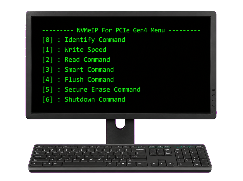
Interactive Serial Console Command Menu
After power-on, the system provides an ASCII command interface through the serial console. Engineers can run full-drive write and read tests, check SMART health information, flush data, issue secure erase commands, and shut down the drive.
🚀 Benchmark Results: Sustained 7,400+ MB/s Full-Disk Transfer
To verify sustained performance without buffer degradation, the test used a random data pattern across the entire 6.4 TB capacity of the enterprise SSD.
| Operation | Interface | Transfer Size | Average Throughput | Peak Throughput | CPU / DDR Required? |
|---|---|---|---|---|---|
| Sequential Write | PCIe Gen4 x4 | 6.4 TB (Full Disk) | 7,421 MB/s | 7,431 MB/s | No / No |
| Sequential Read | PCIe Gen4 x4 | 6.4 TB (Full Disk) | 7,520 MB/s | 7,522 MB/s | No / No |
The performance results show an average write throughput of 7,421 MB/s and an average read throughput of 7,520 MB/s across the full 6.4 TB drive. The measured throughput corresponds to more than 94% of the theoretical PCIe Gen4 x4 bandwidth stated in the source draft.
📌 Use Case Spotlight: Autonomous Vehicle Edge Data Logging
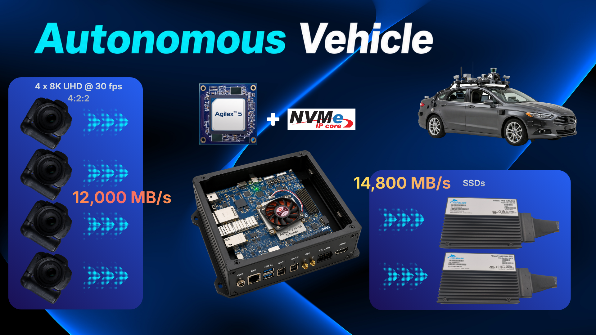
High-resolution ADAS and autonomous vehicle research platforms can generate data rates beyond the capability of a single SSD. As an example, capturing four channels of uncompressed 8K Ultra HD video at 30 FPS in 4:2:2 format requires an aggregate stream of approximately 12,000 MB/s.
By instantiating two independent NVMe-IP cores in one Altera Agilex™ 5 FPGA, developers can build a hardware-level RAID-0 array with two PCIe Gen4 x4 U.2 SSDs.
- Aggregate Write Bandwidth: Up to 14,800 MB/s sustained.
- System Headroom: More than 2,800 MB/s of throughput margin above the 12,000 MB/s camera stream.
- Real-Time Processing: Incoming camera frames can be processed by Agilex™ 5 AI Tensor blocks before direct-to-disk storage within the FPGA-based system.
🔧 Why Choose Design Gateway NVMe-IP?
Design Gateway has developed high-speed storage IP cores for FPGA platforms for more than a decade. NVMe-IP for Altera Agilex™ 5 provides the following engineering advantages:
- Easy, Zero-Cost Start-Up: Begin with a ready-to-run evaluation SOF file and demonstration project for the Agilex™ 5 FPGA board.
- Fully Offloaded Hardware Design: Avoid embedded Linux latency, software driver maintenance, and external DDR4/DDR5 memory controller routing.
- High Performance with Low Resource Usage: Achieve sustained transfer speeds above 7,400 MB/s while using approximately 4,500 ALMs.
- Proven FPGA Storage Technology: Apply Design Gateway storage IP technology to data acquisition, aerospace, defense, medical imaging, and other high-performance applications.
✅ Final Takeaway
Design Gateway NVMe-IP enables direct, deterministic access to PCIe Gen4 NVMe SSDs from Altera Agilex™ 5 FPGA logic. With sustained throughput above 7,400 MB/s, no CPU, and no external DDR memory, the architecture is suitable for high-speed edge recording and real-time data-processing systems that require predictable storage performance.
📩 Contact Us
If you are developing an FPGA-based storage system and would like to discuss whether Design Gateway NVMe-IP is suitable for your application, please contact Design Gateway for more information.
📚 Learn More About NVMe-IP for Altera Agilex™ 5
Explore the related Design Gateway product page and technical documents for more details.
- NVMe-IP Product Page
- NVMe-IP Datasheet
- NVMe-IP Reference Design Document
- NVMe-IP Demo Instruction Document
- NVMe-IP FPGA Board Setup
🧪 Free Evaluation File
Start your evaluation with a reference design and demonstration environment prepared for Design Gateway NVMe-IP on the Altera Agilex™ 5 FPGA platform.
Request a free evaluation package
🤝 Official Partner Platform Availability
Design Gateway provides IP core solutions for leading FPGA platforms, including Intel/Altera FPGA devices. If you are planning to deploy on an Altera platform, our team can help you identify the supported device family, reference design, and evaluation environment that best fits your application.
✅ Altera (FPGA) Partner Solution
Deploy production-ready NVMe storage acceleration on Altera Agilex5 FPGAs with confidence and accelerate your edge storage applications with Design Gateway’s proven NVMe IP Core.