How to Choose the Right FPGA NVMe IP Core: An Application-Driven Selection Guide

Engineered for Pure Hardware Storage Performance: Design Gateway’s all-logic NVMe IP Core family empowers FPGA developers to interface directly with PCIe Gen3, Gen4, and Gen5 NVMe SSDs at wire speed—with zero CPU, zero OS, and zero external DDR RAM overhead.
Why FPGA-Native NVMe? Pure Hardware vs. Conventional Host
Traditional embedded NVMe designs suffer from CPU bottlenecks, OS driver complexity, and non-deterministic latency. Design Gateway replaces the entire software storage stack with a standalone, full-hardware protocol engine inside FPGA logic.
Zero CPU, OS & DDR
- Pure Hardware Engine: Dedicated internal NVMe manager & DMA logic.
- Zero CPU Burden: Completely autonomous operation with no host processor required.
- No External DDR Required: Uses FPGA On-Chip Memory.
Wire-Speed Throughput
- PCIe Gen3 / Gen4 / Gen5 Support: Native support for PCIe Gen3, Gen4, and Gen5 rates.
- 3.0 – 11 GB/s: Single-drive wire speed across Gen3, Gen4, and Gen5.
- Scalable Multi-Drive Performance: Scales up to 40 GB/s with multi-SSD RAID0 array configurations.
Deterministic Latency
- Zero OS Jitter: No kernel paging, cache misses, or interrupt overhead.
- Autonomous State Machine: Full hardware control sequence eliminates CPU driver stack and OS interrupt latencies.
- Real-Time Reliability: Built for radar, aerospace telemetry, LiDAR & edge AI.
Application 1: High-Speed Data Backup & Continuous Streaming
Ideal for high-resolution vision cameras, aerospace flight recorders, radar/RF capture, and medical imaging where high-rate sensor streams must be written sequentially to NVMe storage without dropping a single frame.
Recommended: NVMe IP Core (Standard) & PCIe Soft IP Core
Optimized for single-user sequential read/write operations with minimal FPGA logic utilization.

NVMe IP Core (Standard)
Requires PCIe Hard IP • Lowest Logic Resource Usage

NVMe IP Core with PCIe Soft IP
PCIe Soft IP Included • No PCIe Hard IP Required
Key Architectural Features (Standard)
- Built-in PCIe Hard IP Bridge: Connects directly to the FPGA’s integrated PCIe Hard IP block for lowest LUT and register utilization.
- PCIe Gen3 / Gen4 / Gen5 Support: Scales across PCIe Gen3, Gen4, and Gen5 enterprise SSDs up to 11 GB/s per single drive.
- Sequential Stream Optimization: Dedicated internal DMA and FPGA on-chip memory buffer maximize sustained write/read throughput.
- 512-Byte and 4 KB LBA Support: Supports both 512-byte and 4 KB LBA sector sizes for raw storage access, plus optional FAT32 / exFAT / exFAT2 file system cores (512-byte LBA).
Key Architectural Features (PCIe Soft IP)
- Built-in PCIe Gen3 / Gen4 Soft IP (NVMeG3 / NVMeG4): Implements PCIe protocol layers in logic operating with the FPGA’s PCIe PHY IP—ideal for devices without PCIe Hard IP.
- Preserves Native Hard IP: Frees up the FPGA’s built-in PCIe Hard IP block for host root-complex or upstream backplane links.
- Flexible Multi-Channel RAID0: Enables multi-SSD array expansion across standard high-speed transceiver banks.
- Standalone & PetaLinux Modes: Supports pure-hardware autonomous streaming or hybrid DMA on PetaLinux reference designs.

Hardware Test Bench: AMD Versal™ HBM VHK158 Evaluation Kit paired with PCIe Gen5 Enterprise NVMe SSDs (Micron 9550 & Memblaze PBlaze 7 7946) achieving over 11 GB/s sustained sequential recording.
[Read Full Test Article →]
Related Technical Articles & Deep Dives
•
NVMe-IP Gen5 with Micron 9550 SSD: Achieving Sustained 11 GB/s Write Performance
In-depth empirical validation on AMD Versal VHK158 showcasing sustained sequential throughput and thermal stability.
•
Enable Sustained 11,000 MB/s Recording with DG’s NVMe Gen5 IP & Enterprise SSD
Detailed examination of sustained recording architectures for continuous radar, vision, and raw sensor ingest.
•
Proven NVMe Gen5 Performance with AB19-M2PCI Adapter Board
Hardware adapter solution enabling PCIe Gen5 M.2 SSD connectivity with signal integrity preservation.
Ready-to-Run Evaluation Demos (Standard)
NVMe Performance Test
NVMe Sustain Rate Test
RAID0 x2 / x4 Demo
10G/25GbE FTP Server
Ready-to-Run Evaluation Demos (PCIe Soft IP)
NVMe Performance Test
RAID0 x2 / x4 Demo
DMA on PetaLinux
Application 2: Data Logging with Real-Time Monitoring
Solves a major embedded storage challenge: how to write high-speed sensor streams to SSD while simultaneously reading out previously stored data over 10GbE / 25GbE / 100GbE for real-time monitoring and analytics without interrupting recording.
Recommended: muNVMe IP Core (Multi-User Sequential)
Features built-in multi-channel hardware arbitration supporting 2 to 4 concurrent users with simultaneous Read/Write.

muNVMe IP Core (Multi-User)
2–4 User Channels • Simultaneous Read/Write Arbitration
Simultaneous Read & Write Capabilities
- 2 to 4 Independent User Ports: Supports 4 users (PCIe Gen4) or 2 users (PCIe Gen3) via simple FIFO interfaces—User 0 (Main User) handles control & R/W while Users 1–3 (Sub Users) execute concurrent R/W.
- Simultaneous R/W Streaming: User 0 records live sensor data while User 1 concurrently reads previously recorded data at near-maximum SSD throughput.
- Multi-Queue & Dedicated Per-User Buffer: Built-in multi-queue management with an independent 256 KB or 1 MB FPGA on-chip memory buffer per user implemented 100% in hardware.
- 512-Byte and 4 KB LBA Support: Compatible with both 512-byte and 4 KB LBA sector architectures.
Network Offload Architecture (100GbE)
Pairing with TOE100G-IP Core:
- User 0 (Sensor Ingest): User 0 records live sensor data directly from ADC/LiDAR/Camera into the NVMe SSD.
- User 1 (100GbE FTP Data Path): User 1 concurrently reads previously recorded data for high-speed real-time data access over 100GbE.
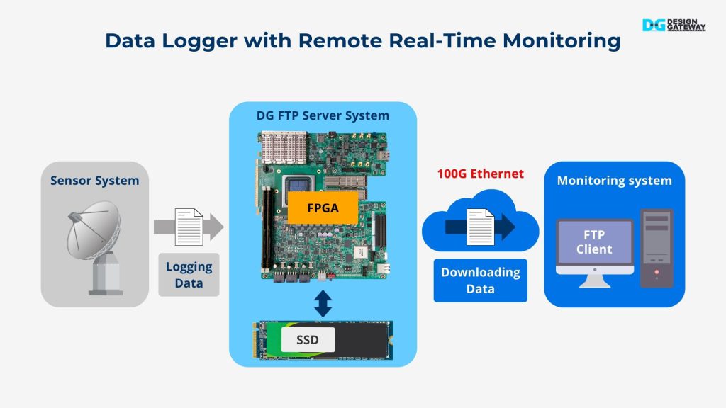
System Architecture: Continuous sensor data logging directly to NVMe SSD while simultaneously serving live data readout via hardware-accelerated FTP data transfer over 100GbE.
[Read Full System Architecture Blog →]
Related Technical Articles & Deep Dives
•
FPGA Data Logging System With Live FTP Monitoring
Comprehensive hardware implementation coupling muNVMe-IP with high-speed FTP server logic for simultaneous record and stream.
•
Case Study: Validating NVMe SSD Sustained Throughput & Buffer Needs for Continuous Data Logging
Empirical validation and buffer right-sizing on AMD Kintex FPGAs to guarantee zero data loss during high-throughput logging.
•
High-Speed File-Based Data Logging for 100G Ethernet Sustained Powered by NVMe-IP for Gen5 and exFAT2-IP
Next-generation 100GbE recording pipeline generating native exFAT files directly readable on host operating systems.
Ready-to-Run Evaluation Demos
NVMe Performance Test Demo
RAID0 x2 Dual-SSD Demo
100GbE FTP Server Network Storage Demo
FAT32 / exFAT / exFAT2 File System Add-on
Application 3: Data Center Applications, Search Engines & Shared Storage
Workloads like search engine index querying, transactional key-value databases, and shared storage caches operate on non-contiguous blocks, demanding hardware-accelerated Random Access with high IOPS and deterministic response times.
Recommended: rmNVMe IP Core & raNVMe IP Core
Engineered specifically for non-sequential, block-level random access with hardware command queue optimization.

rmNVMe IP Core (Random & Multi-User)
Concurrent Access by Two Users • 4 KB Random Access (512-Byte LBA)

raNVMe IP Core (Random Access)
Single-User Dedicated • High IOPS with Low Resource Usage
Key Architectural Features (rmNVMe)
- Concurrent Access by Two Users: 2 independent user interfaces (User 0 for Read/Control and User 1 for Write) operating simultaneously.
- Random Access with 512-Byte LBA: Optimized for 4 KB random read/write transactions on NVMe SSDs using 512-byte logical blocks.
- Configurable Queue Depth (32–256): Independently adjustable Write and Read command depth with 128 KB – 1 MB FPGA on-chip memory buffer.
- Embedded Linux Coexistence: Reference designs bridge hardware-accelerated random access with PetaLinux and Embedded Linux hosts.
Key Architectural Features (raNVMe)
- High IOPS with Low Resource Usage: Streamlined single-user random-access controller achieving >500K random write IOPS without CPU intervention (up to 1.4M Write / 1.3M Read IOPS on VCK190).
- Random Access with 512-Byte LBA: Optimized for 4 KB random read/write transactions on NVMe SSDs using 512-byte logical blocks.
- 32-Command Queue Pipeline: Supports up to 32 Write or Read commands for 4 KB random access with a 128 KB FPGA on-chip memory buffer.
- Deterministic Zero-Jitter Lookups: Bypasses OS file system locks, kernel page caches, and driver interrupts for predictable search queries.
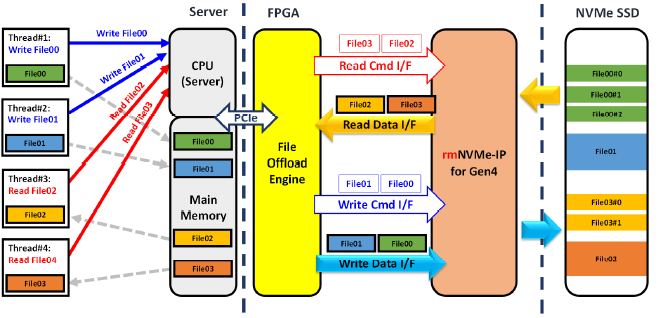
rmNVMe IP Core Architecture: Dual-user concurrent random access allows FPGA query accelerators to execute high-IOPS lookups while the Host CPU updates filesystem tables.
[Read Full Application Note →]
Related Technical Articles & Deep Dives
•
rmNVMe-IP: Random-Access Multi-User NVMe-IP Application
In-depth architecture breakdown of dual-user concurrent random access, independent command queues, and shared memory caching.
•
rmNVMe-IP: Random-Access Multi-User NVMe-IP Demo & Performance
Empirical random IOPS measurements, access latency consistency, and multi-user resource contention benchmarks.
•
Reach 3000 MB/s NVMe SSD with Full Filesystem Access on PetaLinux
Hybrid co-design architecture bridging embedded Linux operating systems with hardware-accelerated NVMe storage pipelines.
Ready-to-Run Evaluation Demos (rmNVMe)
NVMe Performance Test
Random-Access NVMe Host on Embedded Linux
Ready-to-Run Evaluation Demos (raNVMe)
NVMe Performance Test
Data Stream Demo
Multiple User Demo
Storage Throughput Guide: From 3.5 GB/s to 40 GB/s Ultra-Speed
Whether your design relies on a single M.2 PCIe Gen3 SSD or scales to an enterprise 4-channel Gen5 U.2/E1.S RAID0 cluster, Design Gateway provides verified configurations that max out physical interface bandwidth.
3 – 3.5 GB/s
Single-Drive Wire Speed
25% Capacity Scale
1 × SSD
Gen3
3.5 – 7.5 GB/s
High-Speed Streaming & Logging
50% Capacity Scale
1 × SSD
Gen4
2 × SSDs
Gen3
7.5 – 15 GB/s
100GbE Line-Rate Ingest
75% Capacity Scale
1 × SSD
Gen5
2 × SSDs
Gen4
4 × SSDs
Gen3
15 – 40 GB/s
Ultra-Speed Multi-SSD Cluster
100% Max Scale
4 × SSDs
Gen5
2 × SSDs
Gen5
4 × SSDs
Gen4
Comprehensive NVMe IP Core Selection Matrix
Use this side-by-side technical matrix to evaluate user concurrency, sector sizes, bus architectures, and file system add-on compatibility across the entire Design Gateway NVMe selection guide:
| Feature Specification | NVMe IP Core (Standard) |
NVMe IP Core (PCIe Soft IP) |
muNVMe IP Core (Multi-User) |
rmNVMe IP Core (Random Multi-User) |
raNVMe IP Core (Random Single-User) |
|---|---|---|---|---|---|
| User Access | Single user | Single user | 2 – 4 users | 2 users | Single user |
| PCIe IP Requirement | PCIe Hard IP | PCIe Soft IP | PCIe Hard / Soft IP | PCIe Hard / Soft IP | PCIe Hard / Soft IP |
| LBA Sector Sizes | 512-Byte / 4 KB | 512-Byte / 4 KB | 512-Byte / 4 KB | 512-Byte | 512-Byte |
| Sequential Access | ✓ | ✓ | ✓ | ✓ | ✓ |
| Random Access | — | — | — | ✓ | ✓ |
| Simultaneous Write / Read | — | — | ✓ | ✓ | — |
| Multi-SSDs via PCIe Switch | Customization | Customization | — | — | — |
| File System IP (FAT32 / exFAT) (Requires 512-Byte LBA) |
✓ | ✓ | ✓ | — | — |
| Product Links |
Broad FPGA Family Device Support
Design Gateway NVMe IP cores are validated across AMD and Altera device families, spanning legacy 7-series to state-of-the-art FinFET & 3D chiplet platforms:
AMD FPGA & Adaptive SoC Devices
Versal HBM / Premium / AI
Alveo Accelerator Cards
Virtex UltraScale+
Zynq UltraScale+ (MPSoC / RFSoC)
Kintex UltraScale+ / Artix UltraScale+
Kintex UltraScale
Kintex-7 / Virtex-7 / Artix-7
Zynq-7000 SoC
Altera FPGA & SoC Devices
Agilex 7 (I-Series / F-Series)
Agilex 5 (E-Series)
Stratix 10 GX
Arria 10 SoC / Arria 10 GX
Cyclone 10 GX
Arria V GX
Turnkey Ecosystem: Hardware File Systems & Network Offload Engines
Design Gateway offers a complete modular IP ecosystem designed to connect directly with NVMe storage pipelines without introducing CPU overhead:
FAT32 & exFAT / exFAT2 IP
Pure hardware file system management cores that create real-time PC-compatible files and directory structures on NVMe SSDs. Operators can eject the SSD and open recorded files instantly in Windows, macOS, or Linux.
NVMe IP Switch Core
Enables an FPGA to orchestrate and multiplex across multiple downstream NVMe SSDs through standard PCIe switch ICs or multichannel PCIe links, providing effortless drive expansion.
TOE Network Offload (10GbE / 25GbE / 100GbE)
Hardware-accelerated FTP file transfers using TOE100G-IP, exFAT2-IP, and muNVMe-IP, with CPU-independent high-speed data transfer.
Accelerate Your FPGA NVMe Storage Development
Eliminate CPU development overhead, simplify board routing with zero external DDR, and achieve wire-speed PCIe Gen3, Gen4, or Gen5 storage performance. Request ready-to-run evaluation demo bitfiles and test on standard development boards today.